Application information – Rainbow Electronics MAX3420E User Manual
Page 15

In full-duplex mode (FDUPSPI=1), the MOSI and MISO
pins are separate, and the MISO pin drives only when
SS
is low. In this mode, the first eight SCLK edges (after
SS =
0) clock the command byte into the MAX3420E on MOSI,
and eight USB status bits are clocked out of the
MAX3420E on MISO. For an SPI write cycle, any bytes
following the command byte are clocked into the
MAX3420E on MOSI, and zeros are clocked out on MISO.
For an SPI read cycle, any bytes following the command
byte are clocked out of the MAX3420E on MISO and the
data on MOSI is ignored. At the conclusion of the SPI
cycle (
SS = 1), the MISO output tri-states.
In half-duplex mode, the MOSI pin is a bidirectional pin
and the MISO pin is tri-stated. This saves a pin in the SPI
interface. Because of the shared data pin, this mode
does not offer the eight USB status bits (Figure 5) as the
command byte is clocked into the MAX3420E. The MISO
pin can be left unconnected in half-duplex mode.
SCLK (Serial Clock)
The SPI master provides the MAX3420E SCLK signal to
clock the SPI interface. SCLK has no low-frequency limit,
and can be as high as 26MHz. The MAX3420E changes
its output data (MISO) on the falling edge of SCLK and
samples input data (MOSI) on the rising edge of SCLK.
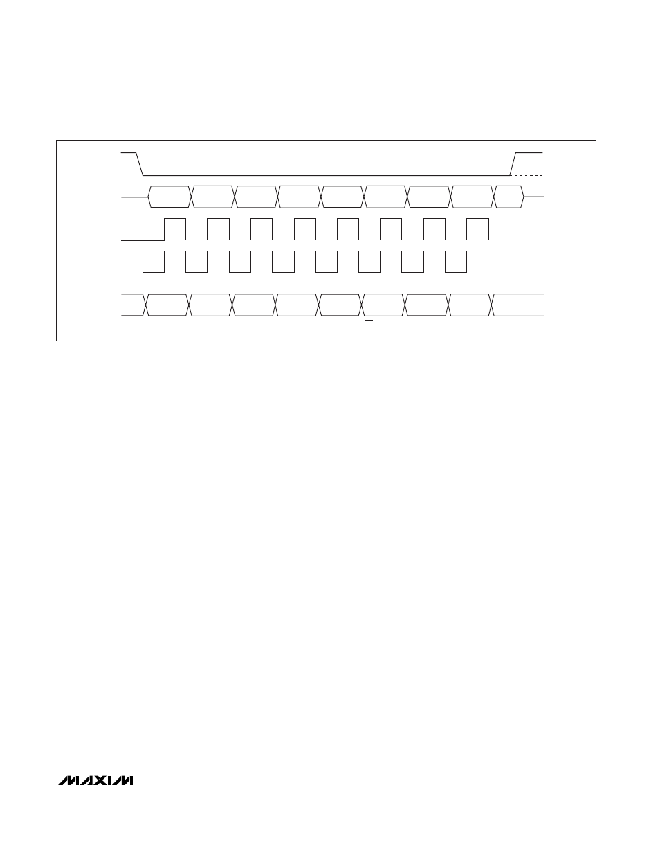
The MAX3420E ignores SCLK transitions when
SS is
high. The inactive level of SCLK may be low or high,
depending on the SPI operating mode (Figure 14).
SS
(Slave Select)
The MAX3420E SPI interface is active only when
SS is
low. When
SS is high, the MAX3420E tri-states the SPI
output pin and resets the internal MAX3420 SPI logic. If
SS goes high before a complete byte is clocked in, the
byte-in-progress is discarded. The SPI master can ter-
minate an SPI cycle after clocking in the first 8 bits (the
command byte). This feature can be used in a full-
duplex system to retrieve the USB status bits (Figure 5)
without sending or receiving SPI data. The MAX3420E
SS pin is sensitive to undershoot. A 33pF capacitor
should be connected from the
SS pin to ground to pre-
vent any noise spikes.*
Application Information
SPI Interface
The MAX3420E operates as an SPI slave device. A reg-
ister access consists of the SPI master first writing an
SPI command byte, followed by reading or writing the
contents of the addressed register (see the Register
Description section for more detail). All SPI transfers
are MSB (most significant bit) first. The external SPI
master provides a clock signal to the MAX3420E SCLK
input. This clock frequency can be between DC and
26MHz. Bit transfers occur on the positive edge of
SCLK. The MAX3420E counts bits and divides them
into bytes. If fewer than 8 bits are clocked into the
MAX3420E when
SS goes high, the MAX3420E dis-
cards the partial byte.
The MAX3420E SPI interface operates without adjust-
ment in either SPI mode (CPOL = 0, CPHA = 0) or
(CPOL = 1, CPHA = 1). No mode bit is required to
select between the two modes since the interface uses
the rising edge of the clock in both modes. The two
clocking modes are illustrated in Figure 14. Note that
the inactive SCLK value is different for the two modes.
Figure 14 illustrates the full-duplex mode, where data is
simultaneously clocked into and out of the MAX3420E.
MAX3420E
USB Peripheral Controller
with SPI Interface
______________________________________________________________________________________
15
SS
MISO
MOSI
SCLK
MODE 0,0
SCLK
MODE 1,1
SPI MODE 0,0 OR 1,1
* MSB OF NEXT BYTE IN BURST MODE (SS REMAINS LOW)
Q7
Q6
Q5
Q4
Q3
D7
D6
D5
D4
D3
D2
D1
D0
*
Q2
Q1
Q0
*
Figure 14. SPI Clocking Modes
*33pF capacitor will not be required after redesign.
