Rainbow Electronics MAX106 User Manual
Page 25

MAX106
±5V, 600Msps, 8-Bit ADC with On-Chip
2.2GHz Bandwidth Track/Hold Amplifier
______________________________________________________________________________________
25
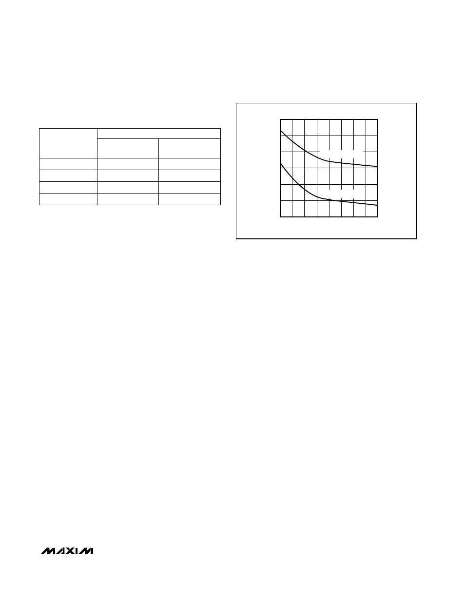
Thermal Performance
The MAX106 has been modeled to determine the thermal
resistance from junction to ambient. Table 7 lists the
ADC’s thermal performance:
Ambient Temperature:
T
A
= +70°C
Heatsink Dimensions:
25mm x 25mm x 10mm
PC Board Size and Layout:
4in. x 4in.
2 Signal Layers
2 Power Layers
Heatsink Manufacturers
Aavid Engineering and IERC provide open-tooled, low-
profile heatsinks, fitting the 25mm x 25mm ESBGA
package.
Aavid Engineering, Inc.
Phone: 714-556-2665
Heatsink Catalog No.: 335224B00032
Heatsink Dimensions: 25mm x 25mm x 10mm
International Electronic Research Corporation (IERC)
Phone: 818-842-7277
Heatsink Catalog No.: BDN09-3CB/A01
Heatsink Dimensions: 23.1mm x 23.1mm x 9mm
Bypassing/Layout/Power Supply
Grounding and power-supply decoupling strongly influ-
ence the MAX106’s performance. At 600MHz clock fre-
quency and 8-bit resolution, unwanted digital crosstalk
may couple through the input, reference, power-supply,
and ground connections and adversely influence the
dynamic performance of the ADC. Therefore, closely
follow the grounding and power-supply decoupling
guidelines (Figure 22).
Maxim strongly recommends using a multilayer printed
circuit board (PCB) with separate ground and power-
supply planes. Since the MAX106 has separate analog
and digital ground connections (GNDA, GNDI, GNDR,
and GNDD, respectively), the PCB should feature sep-
arate analog and digital ground sections connected at
only one point (star ground at the power supply). Digital
signals should run above the digital ground plane, and
analog signals should run above the analog ground
plane. Keep digital signals far away from the sensitive
analog inputs, reference inputs, and clock inputs. High-
speed signals, including clocks, analog inputs, and
digital outputs, should be routed on 50
Ω microstrip
lines such as those employed on the MAX106 evalua-
tion kit.
The MAX106 has separate analog and digital power-
supply inputs: V
EE
(-5V analog and substrate supply)
and V
CC
I (+5V) to power the T/H amplifier, clock distri-
bution, bandgap reference, and reference amplifier;
V
CC
A (+5V) to supply the ADC’s comparator array;
V
CC
O (+3V to V
CC
D) to establish power for all PECL-
based circuit sections; and V
CC
D (+5V) to supply all
logic circuits of the data converter.
The MAX106 V
EE
supply contacts must not be left
open while the part is being powered up. To avoid this
condition, add a high-speed Schottky diode (such as a
Motorola 1N5817) between V
EE
and GNDI. This diode
prevents the device substrate from forward biasing,
which could cause latchup.
Table 7. Thermal Performance for
MAX106 With or Without Heatsink
16.5
0
12.5
14.3
9.4
200
13
8.3
400
12.5
7.4
800
6
8
10
12
14
16
18
0
200
100
300 400 500 600 700 800
THERMAL RESISTANCE vs. AIRFLOW
AIRFLOW (linear ft./min.)
θ
JA
(°
C/W)
WITH HEATSINK
WITHOUT HEATSINK
Figure 21. MAX106 Thermal Performance
MAX106
θ
JA
(°C/W)
WITHOUT
HEATSINK
WITH HEATSINK
AIRFLOW
(linear ft/min)
