Rainbow Electronics MAX106 User Manual
Page 13
MAX106
±5V, 600Msps, 8-Bit ADC with On-Chip
2.2GHz Bandwidth Track/Hold Amplifier
______________________________________________________________________________________
13
Principle of Operation
The MAX106’s flash or parallel architecture provides
the fastest multibit conversion of all common integrated
ADC designs. The key to this high-speed flash archi-
tecture is the use of an innovative, high-performance
comparator design. The flash converter and down-
stream logic translate the comparator outputs into a
parallel 8-bit output code and pass this binary code on
to the optional 8:16 demultiplexer, where primary and
auxiliary ports output PECL-compatible data at up to
300Msps per port (depending on how the demultiplex-
er section is set on the MAX106). The ideal transfer
function appears in Figure 2.
On-Chip Track/Hold Amplifier
As with all ADCs, if the input waveform is changing
rapidly during conversion, ENOB and signal-to-noise
ratio (SNR) specifications will degrade. The MAX106’s
on-chip, wide-bandwidth (2.2GHz) T/H amplifier reduces
this effect and increases the ENOB performance signifi-
cantly, allowing precise capture of fast analog data at
high conversion rates.
The T/H amplifier buffers the input signal and allows a
full-scale signal input range of ±250mV. The T/H ampli-
fier’s differential 50
Ω input termination simplifies inter-
facing to the MAX106 with controlled impedance lines.
Figure 3 shows a simplified diagram of the T/H amplifier
stage internal to the MAX106.
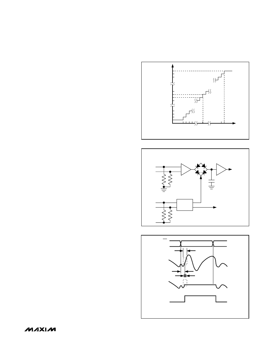
Aperture width, delay, and jitter (or uncertainty) are
parameters that affect the dynamic performance of
high-speed converters. Aperture jitter, in particular,
directly influences SNR and limits the maximum slew
rate (dV/dt) that can be digitized without a significant
contribution of errors. The MAX106’s innovative T/H
amplifier design typically limits aperture jitter to less
than 0.5ps.
Aperture Width
Aperture width (t
AW
) is the time the T/H circuit requires
(Figure 4) to disconnect the hold capacitor from the
input circuit (for instance to turn off the sampling bridge
and put the T/H unit in hold mode).
Aperture Jitter
Aperture jitter (t
AJ
) is the sample-to-sample variation
(Figure 4) in the time between the samples.
Aperture Delay
Aperture delay (t
AD
) is the time defined between the
rising edge of the sampling clock and the instant when
an actual sample is taken (Figure 4).
(-FS + 1LSB)
0
(+FS - 1LSB)
+FS
OVERRANGE + 255
255
254
129
128
127
126
3
2
1
0
ANALOG INPUT
DIGITAL OUTPUT
TO
COMPARATORS
TO
COMPARATORS
BUFFER
AMPLIFIER
INPUT
AMPLIFIER
CLOCK
SPLITTER
ALL INPUTS ARE ESD PROTECTED
(NOT SHOWN IN THIS
SIMPLIFIED DRAWING).
SAMPLING
BRIDGE
GNDI
50
Ω
50
Ω
VIN+
VIN-
GNDI
C
HOLD
50
Ω
50
Ω
CLK+
CLK-
CLKCOM
Figure 3. Internal Structure of the 2.2GHz T/H Amplifier
HOLD
CLK
ANALOG
INPUT
SAMPLED
DATA (T/H)
T/H
t
AW
t
AD
t
AJ
TRACK
TRACK
APERTURE DELAY (t
AD
)
APERTURE WIDTH (t
AW
)
APERTURE JITTER (t
AJ
)
CLK
Figure 4. T/H Aperture Timing
Figure 2. Transfer Function