Table 5. dc-coupled clock drive options – Rainbow Electronics MAX106 User Manual
Page 20

MAX106
±5V, 600Msps, 8-Bit ADC with On-Chip
2.2GHz Bandwidth Track/Hold Amplifier
20
______________________________________________________________________________________
AC-Coupling Clock Inputs
The clock inputs CLK+ and CLK- can also be driven
with positive referenced ECL (PECL) logic levels if the
clock inputs are AC-coupled. Under this condition, con-
nect CLKCOM to GNDI. Single-ended ECL/PECL/sine-
wave drive is also possible if the undriven clock input is
reverse-terminated to GNDI through a 50
Ω resistor in
series with a capacitor whose value is identical to that
used to couple the driven input.
Demux Reset Operation
The MAX106 features an internal 1:2 demultiplexer that
reduces the data rate of the output digital data to one-
half the sample clock rate. Demux reset is necessary
when interleaving multiple MAX106s and/or synchroniz-
ing external demultiplexers. The simplified block dia-
gram of Figure 1 shows that the demux reset signal path
consists of four main circuit blocks. From input to out-
put, they are the reset input dual latch, the reset
pipeline, the demux clock generator, and the reset out-
put. The signals associated with the demux reset opera-
tion and the control of this section are listed in Table 6.
Reset Input Dual Latch
The reset input dual-latch circuit block accepts differ-
ential PECL reset inputs referenced to the same V
CC
O
power supply that powers the MAX106 PECL outputs.
For applications that do not require a synchronizing
reset, the reset inputs can be left open. In this case,
they will self-bias to a proper level with internal 50k
Ω
resistors and a 20µA current source. This combination
creates a -1V difference between RSTIN+ and RSTIN-
to disable the internal reset circuitry. When driven with
PECL logic levels terminated with 50
Ω to (V
CC
O - 2V),
the internal biasing network can easily be overdriven.
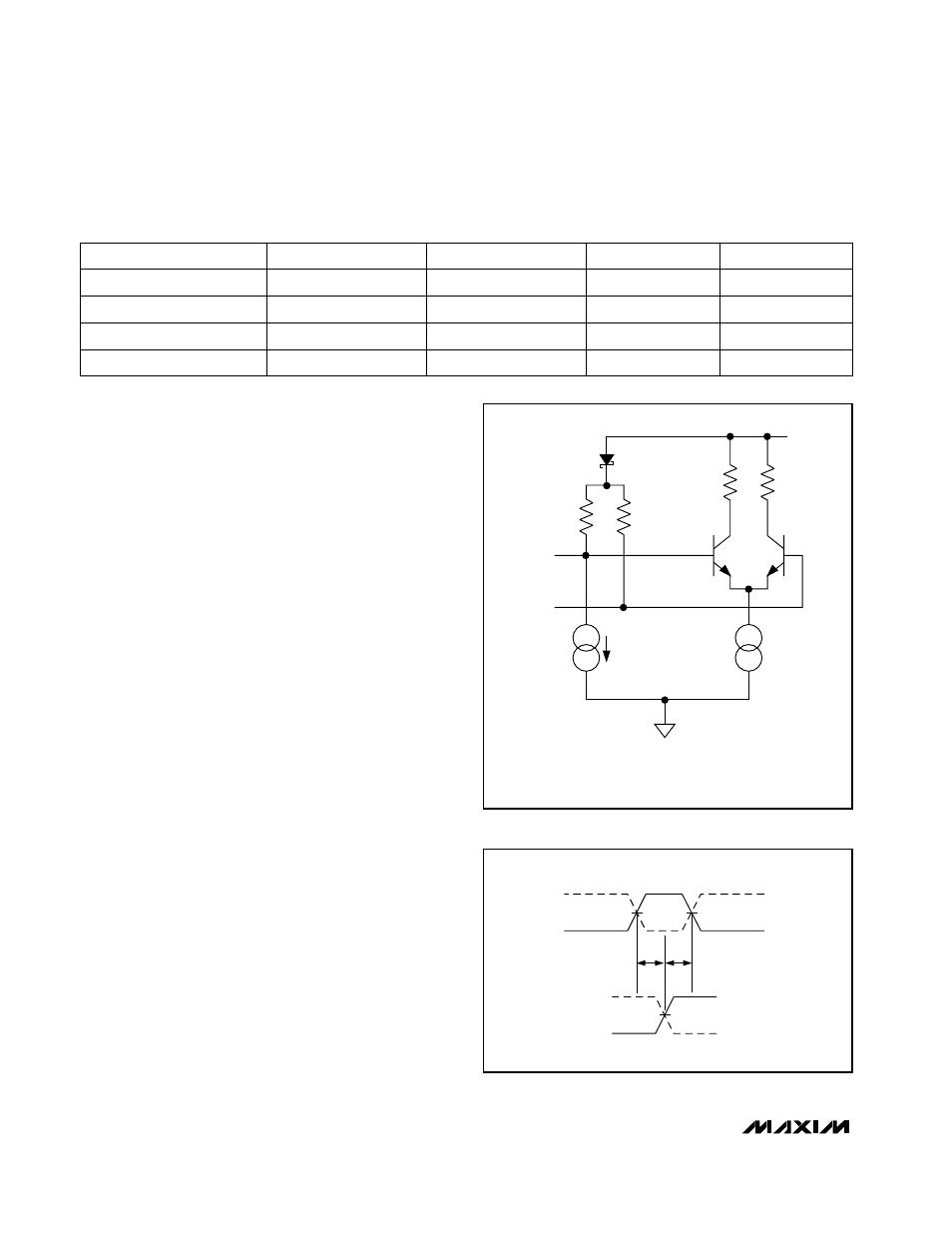
Figure 14 shows a simplified schematic of the reset
input structure.
To properly latch the reset input data, setup (t
SU
) and
data-hold times (t
HD
) must be met with respect to the
rising edge of the sample clock. The timing diagram of
Figure 15 shows the timing relationship of the reset
input and sampling clock.
Table 5. DC-Coupled Clock Drive Options
-10dBm to +4dBm
Figure 13a
Single-Ended Sine Wave
CLK+
GNDI
CLKCOM
CLOCK DRIVE
REFERENCE
External 50
Ω to GNDI
CLK-
-10dBm to +4dBm
-10dBm to +4dBm
Figure 13b
Differential Sine Wave
GNDI
ECL Drive
-1.3V
Figure 13c
Single-Ended ECL
-2V
ECL Drive
ECL Drive
Figure 13d
Differential ECL
-2V
50k
50k
RSTIN+
RSTIN-
RESET INPUTS ARE ESD PROTECTED
(NOT SHOWN ON THIS SIMPLIFIED DRAWING).
20
µA
GNDD
V
CC
O
Figure 14. Simplified Reset Input Structure
RSTIN+
50%
50%
CLK+
CLK-
RSTIN-
50%
t
SU
t
HD
Figure 15. Reset Input Timing Definitions
