Table 1. pecl output functions – Rainbow Electronics MAX106 User Manual
Page 14

MAX106
±5V, 600Msps, 8-Bit ADC with On-Chip
2.2GHz Bandwidth Track/Hold Amplifier
14
______________________________________________________________________________________
Internal Reference
The MAX106 features an on-chip +2.5V precision
bandgap reference that can be used by connecting
REFOUT to REFIN. This connects the reference output
to the positive input of the reference buffer. The buffer’s
negative input is internally tied to GNDR. GNDR must
be connected to GNDI on the user’s application board.
REFOUT can source up to 2.5mA to supply external
devices if required.
An adjustable external reference can be used to adjust
the ADC’s full-scale range. To use an external refer-
ence supply, connect a high-precision reference to the
REFIN pin and leave the REFOUT pin floating. In this
configuration, REFOUT must not be simultaneously
connected at any time, to avoid conflicts between the
two references. REFIN has a typical input resistance of
5k
Ω and accepts input voltages of +2.5V ±200mV.
Using the MAX106’s internal reference is recommend-
ed for best performance.
Digital Outputs
The MAX106 provides data in offset binary format to dif-
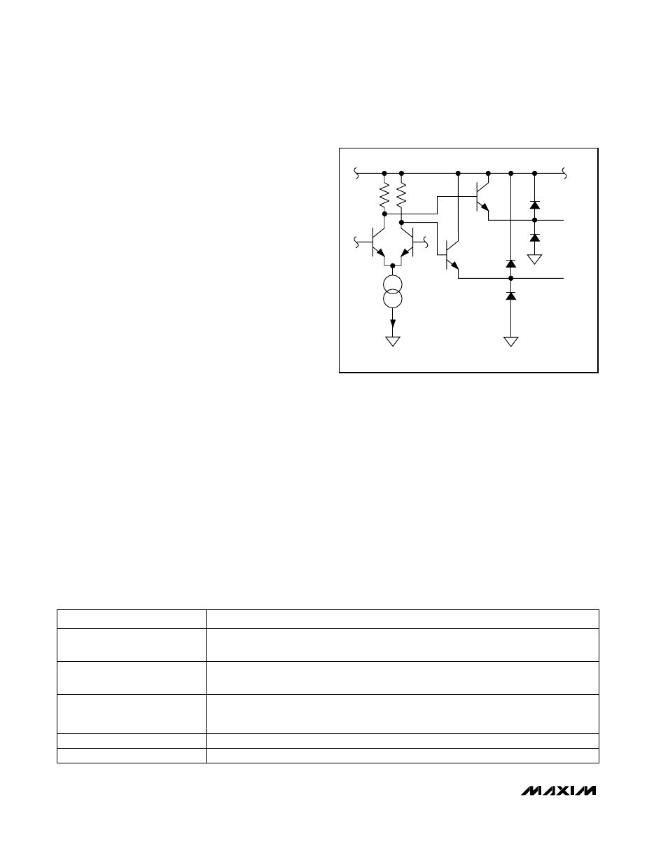
ferential PECL outputs. A simplified circuit schematic of
the PECL output cell is shown in Figure 5. All PECL out-
puts are powered from V
CC
O, which may be operated
from any voltage between +3.0V to V
CC
D for flexible
interfacing with either +3.3V or +5V systems. The nomi-
nal V
CC
O supply voltage is +3.3V.
All PECL outputs on the MAX106 are open-emitter
types and must be terminated at the far end of each
transmission line with 50
Ω to V
CC
O - 2V. Table 1 lists all
MAX106 PECL outputs and their functions.
Demultiplexer Operation
The MAX106 features an internal data demultiplexer,
which provides for three different modes of operation
(see the following sections on Demultiplexed DIV2
Mode, Non-Demultiplexed DIV1 Mode, and Decimation
DIV4 Mode) controlled by two TTL/CMOS-compatible
inputs: DEMUXEN and DIVSELECT.
DEMUXEN enables or disables operation of the internal
1:2 demultiplexer. A logic high on DEMUXEN activates
the internal demultiplexer, and a logic low deactivates
it. With the internal demultiplexer enabled, DIVSELECT
controls the selection of the operational mode. DIVSE-
LECT low selects demultiplexed DIV2 mode, and DIV-
SELECT high selects decimation DIV4 mode (Table 2).
Auxiliary-Port Differential Outputs from LSB to MSB. A “+” indicates the true value; a “-”
denotes the complementary outputs.
A0+ to A7+,
A0- to A7-
Overrange True and Complementary Outputs
OR+, OR-
Data-Ready Clock True and Complementary Outputs. These signal lines are used to latch
the output data from the primary to the auxiliary output ports. Data changes on the rising
edge of the DREADY clock.
DREADY+, DREADY-
Reset Output True and Complementary Outputs
RSTOUT+, RSTOUT-
PECL OUTPUT SIGNALS
Primary-Port Differential Outputs from LSB to MSB. A “+” indicates the true value; a “-”
denotes the complementary outputs.
P0+ to P7+,
P0- to P7-
FUNCTION
DIFF.
PAIR
500
Ω
500
Ω
1.8mA
GNDD
GNDD
GNDD
V
CC
O
A_+/P_+
A_-/P_-
Figure 5. Simplified PECL Output Structure
Table 1. PECL Output Functions
