3v supply ac electrical characteristic – Rainbow Electronics MAX2063 User Manual
Page 5
MAX2063
Dual 50MHz to 1000MHz High-Linearity,
Serial/Parallel-Controlled Digital VGA
5
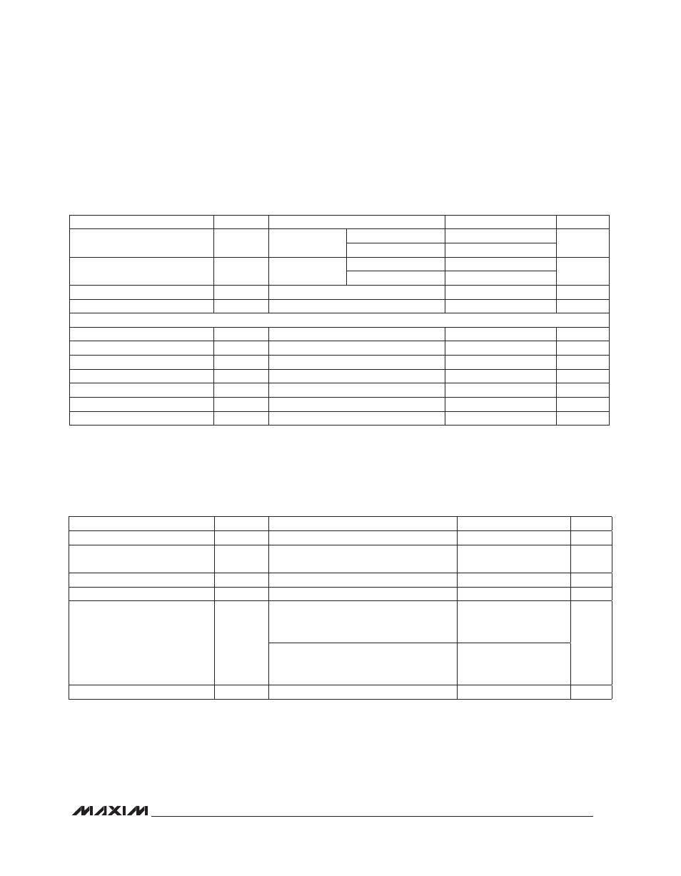
+5V SUPPLY AC ELECTRICAL CHARACTERISTICS (continued)
(Typical Application Circuit, V
CC
= V
CC_AMP_1
= V
CC_AMP_2
= V
CC_RG
= +4.75V to +5.25V, attenuators are set for maximum gain,
RF ports are driven from 50I sources, AMPSET = 0, PD_1 = PD_2 = 0, 100MHz
≤ f
RF
≤ 500MHz, T
C
= -40NC to +85NC. Typical
values are at maximum gain setting, V
CC_
= +5.0V, P
IN
= -20dBm, f
RF
= 350MHz, and T
C
= +25NC, unless otherwise noted.) (Note 6)
+3.3V SUPPLY AC ELECTRICAL CHARACTERISTIC
(Typical Application Circuit, V
CC
= V
CC_AMP_1
= V
CC_AMP_2
= V
CC_RG
= +3.3V, attenuators are set for maximum gain, RF ports
are driven from 50I sources, AMPSET = 1, PD_1 = PD_2 = 0, 100MHz
≤ fRF ≤ 500MHz, T
C
= -40NC to +85NC. Typical values are at
maximum gain setting, V
CC_
= +3.3V, P
IN
= -20dBm, f
RF
= 350MHz, and T
C
= +25NC, unless otherwise noted.) (Note 6)
Note 5: Operation outside this range is possible, but with degraded performance of some parameters. See the Typical Operating
Characteristics.
Note 6: All limits include external component losses. Output measurements are performed at the RF output port of the Typical
Application Circuit.
Note 7: It is advisable not to continuously operate RF input 1 or RF input 2 above +15dBm.
PARAMETER
SYMBOL
CONDITIONS
MIN
TYP
MAX
UNITS
Amplitude Overshoot/
Undershoot
Between any
two states
Elapsed time = 15ns
1.0
dB
Elapsed time = 40ns
0.05
Switching Speed
RF settled to
within Q0.1dB
31dB to 0dB
25
ns
0dB to 31dB
21
Input Return Loss
RL
IN
50I source
21.6
dB
Output Return Loss
RL
OUT
50I load
21.2
dB
SERIAL PERIPHERAL INTERFACE (SPI)
Maximum Clock Speed
f
CLK
20
MHz
Data-to-Clock Setup Time
t
CS
2
ns
Data-to-Clock Hold Time
t
CH
2.5
ns
Clock-to-CS Setup Time
t
ES
3
ns
CS Positive Pulse Width
t
EW
7
ns
CS Setup Time
t
EWS
3.5
ns
Clock Pulse Width
t
CW
5
ns
PARAMETER
SYMBOL
CONDITIONS
MIN
TYP
MAX
UNITS
Small-Signal Gain
G
20.9
dB
Output Third-Order Intercept
Point
OIP3
P
OUT
= 0dBm/tone
29.6
dBm
Noise Figure
NF
5.9
dB
Total Attenuation Range
30.8
dB
Path Isolation
RF input 1 amplified power measured at
RF output 2 relative to RF output 1, all
unused ports terminated to 50I
48.8
dB
RF input 2 amplified power measured at
RF output 1 relative to RF output 2, all
unused ports terminated to 50I
49.1
Output -1dB Compression Point
P
1dB
(Note 7)
13.4
dBm