Detailed description, Applications information, Table 1. control logic table 2. operating modes – Rainbow Electronics MAX2063 User Manual
Page 15
MAX2063
Dual 50MHz to 1000MHz High-Linearity,
Serial/Parallel-Controlled Digital VGA
15
Detailed Description
The MAX2063 high-linearity digital VGA is a general-
purpose, high-performance amplifier designed to
interface with 50I systems operating in the 50MHz to
1000MHz frequency range. Each channel of the device
integrates one digital attenuator to provide 31dB of total
gain control, as well as a driver amplifier optimized to
provide high gain, high output IP3, low NF, and low
power consumption.
Each digital attenuator is controlled as a slave
peripheral using either the SPI-compatible interface or
a 5-bit parallel bus with 31dB total adjustment range
in 1dB steps. An added feature allows “rapid-fire” gain
selection between each of four steps, preprogrammed
by the user through the SPI-compatible interface. A
separate 2-pin control allows the user to quickly access
any one of four customized attenuation states without
reprogramming the SPI bus.
Because each of the two stages in the separate
signal paths has its own RF input and RF output, this
component can be configured to either optimize NF
(amplifier configured first) or OIP3 (amplifier configured
last). The device’s performance features include 24dB
of amplifier gain (amplifier only), 5.6dB NF at maximum
gain (includes attenuator insertion losses), and a high
OIP3 level of +41dBm. Each of these features makes
the device an ideal VGA for multipath receiver and
transmitter applications.
5-Bit Digital Attenuator Control
The device integrates two 5-bit digital attenuators to
achieve a high level of dynamic range. Each digital
attenuator has a 31dB control range, a 1dB step size,
and can be programmed either through a dedicated
5-bit parallel bus or through the 3-wire SPI. See the
Applications Information section and Table 1 for attenu-
ator programming details. The attenuators can be used
for both static and dynamic power control.
Driver Amplifiers
The device includes two high-performance drivers with
a fixed gain of 24dB. Each driver amplifier circuit is
optimized for high linearity for the 50MHz to 1000MHz
frequency range.
Applications Information
Operating Modes
The device features an optional +3.3V supply voltage oper-
ation with reduced linearity performance. The AMPSET pin
needs to be biased accordingly in each mode, as listed in
Table 2. In addition, the driver amplifiers can be shut down
independently to conserve DC power. See the biasing
scheme outlined in Table 2 for details.
SPI Interface and Attenuator Settings
The attenuators can be programmed through the 3-wire
SPI/MICROWIREK-compatible serial interface using
5-bit words. Fifty-six bits of data are shifted in MSB first
and framed by CS. The first 28 bits set the first attenua-
tor, and the following 28 bits set the second attenuator.
When CS is low, the clock is active and data is shifted on
the rising edge of the clock. When CS transitions high,
the data is latched and the attenuator setting changes
(Figure 1). See Table 3 for details on the SPI data format.
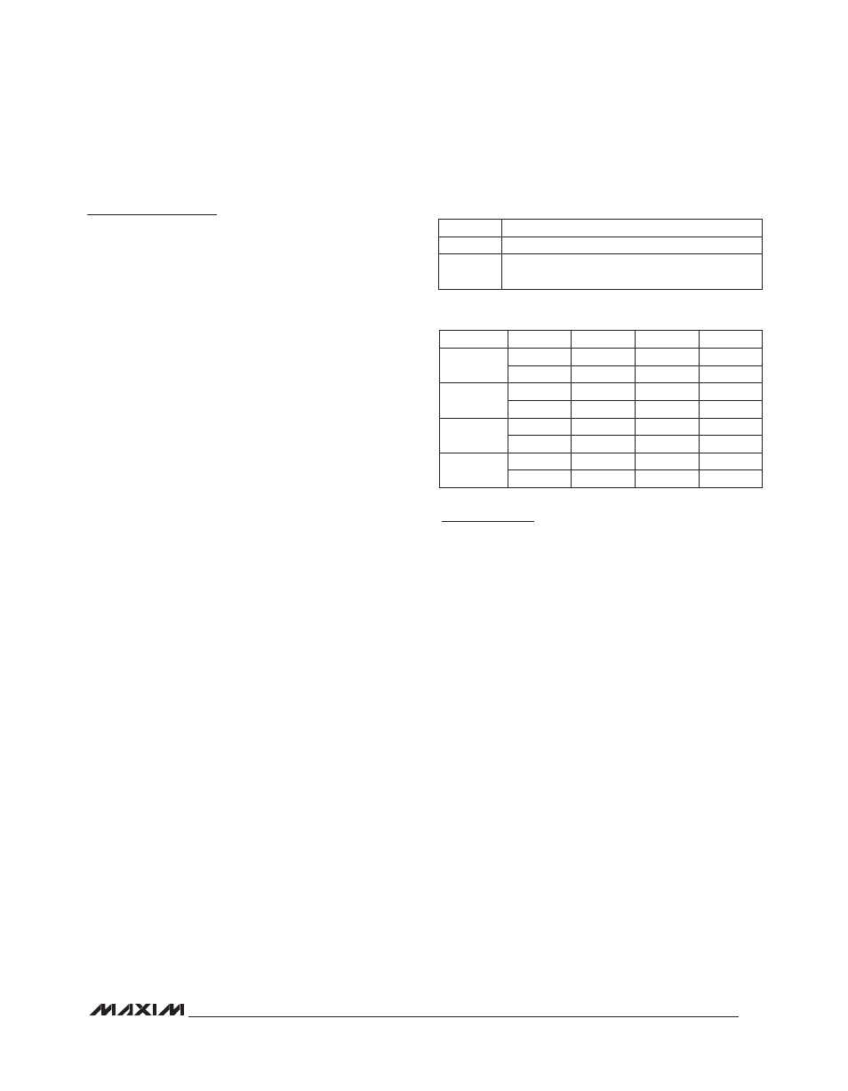
Table 1. Control Logic
Table 2. Operating Modes
MICROWIRE is a trademark of National Semiconductor Corp.
DA_SP
DIGITAL ATTENUATOR
0
Parallel controlled
1
SPI controlled (control voltages show up on the
parallel control pins)
RESULT
V
CC_
(V)
AMPSET
PD_1
PD_2
All on
5
0
0
0
3.3
1
0
0
AMP1 off
AMP2 on
5
0
1
0
3.3
1
1
0
AMP1 on
AMP2 off
5
0
0
1
3.3
1
0
1
All off
5
0
1
1
3.3
1
1
1