Rainbow Electronics MXL1116 User Manual
General description, Applications, Features

_______________General Description
The Maxim MXL1016 (10ns typ) and MXL1116 (12ns
typ) high-speed, complementary-output comparators
are designed specifically to interface directly to TTL
logic while operating from either a dual ±5V supply or a
single +5V supply.
The MXL1016/MXL1116 remain stable with the outputs
in the active region, which greatly reduces output insta-
bility common with slow-moving input signals. In addi-
tion, an output latch (LE) is provided.
For lower-power, higher-performance comparators, see
the MAX912/MAX913 dual/single comparator data
sheet. The MAX913 is an improved, plug-in replace-
ment for the MXL1016 and MXL1116, and the MAX912
is the dual equivalent to the MAX913.
________________________Applications
High-Speed A/D Converters
Zero-Crossing Detectors
Current Sense for Switching Regulators
High-Speed Sampling Circuits
High-Speed Triggers
Line Receivers
Extended Range V/F Converters
Fast Pulse Height/Width Discriminators
____________________________Features
♦
Ultra Fast (10ns typ)
♦
Single +5V or Dual ±5V Supply Operation
♦
Input Common-Mode Extends to
Negative Supply (MXL1116)
♦
Inputs Can Exceed the Positive Supply
Up to +15V (MXL1116) Without Damage
♦
Complementary TTL Outputs
♦
Low Offset Voltage:
1mV
♦
No Minimum Input Slew-Rate Requirement
♦
No Power-Supply Current Spiking
♦
Output Latch
______________Ordering Information
MXL1016/MXL1116
Ultra-Fast Precision TTL Comparators
________________________________________________________________
Maxim Integrated Products
1
1
2
3
4
8
7
6
5
V+
IN+
IN–
V–
QOUT
QOUT
GND
LE
DIP/SO
MXL1016/MXL1116
+
-
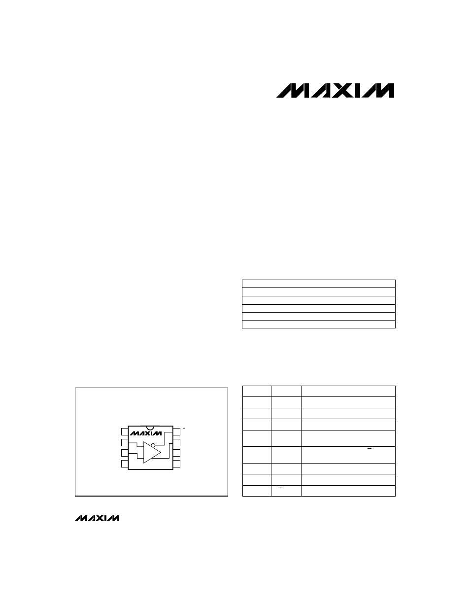
__________________Pin Configuration
_____________________Pin Description
Call toll free 1-800-998-8800 for free samples or literature.
19-0138; Rev. 2; 4/95
PART
TEMP. RANGE
PIN-PACKAGE
MXL1016
CN8
0°C to +70°C
8 Plastic DIP
MXL1016CS8
0°C to +70°C
8 SO
MXL1016MJ8
–55°C to +125°C
8 CERDIP
MXL1116
CN8
0°C to +70°C
8 Plastic DIP
MXL1116CS8
0°C to +70°C
8 SO
TOP VIEW
PIN
NAME
FUNCTION
1
V+
Positive Power Supply, +5V
2
IN+
Noninverting Input
3
IN-
Inverting Input
4
V-
Negative Power Supply, -5V for dual
supply or GND for single supply
5
LE
Latch Enable, QOUT and QOUT are
latched when LE is high
6
GND
Ground
7
QOUT
TTL Output
8
QOUT
Complementary TTL Output
