Pin description – Rainbow Electronics MAX510 User Manual
Page 8
MAX509/MAX510
Quad, Serial 8-Bit DACs
with Rail-to-Rail Outputs
8
_______________________________________________________________________________________
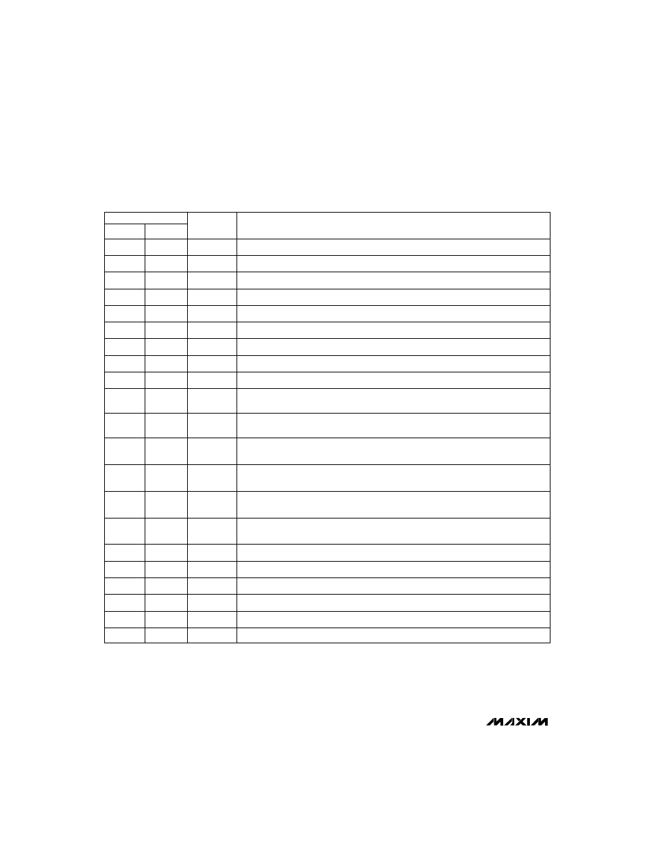
NAME
FUNCTION
1
OUTB
DAC B Voltage Output
2
OUTA
DAC A Voltage Output
3
V
SS
Negative Power Supply, 0V to -5V ±10%. Connect to AGND for single-supply operation.
PIN
MAX509
MAX510
1
2
4
REFB
Reference Voltage Input for DAC B
–
REFAB
Reference Voltage Input for DACs A and B
5
REFA
Reference Voltage Input for DAC A
6
AGND
Analog Ground
3
–
4
7, 14
N.C.
Not Internally Connected
8
DGND
Digital Ground
–
5
–
6
______________________________________________________________Pin Description
10
DOUT
8
9
LDAC
7
11
CLR
9
12
DIN
10
13
SCLK
11
15
CS
12
16
REFD
Reference Voltage Input for DAC D
–
–
REFCD
Reference Voltage Input for DACs C and D
13
Load DAC Input (active low). Driving this asynchronous input low (level sensitive)
transfers the contents of each input latch to its respective DAC latch.
Serial Data Output. Can sink and source current. Data at DOUT is adjustable to be
clocked out on rising or falling edge of SCLK.
17
REFC
Reference Voltage Input for DAC C
–
18
V
DD
Positive Power Supply, +5V ±10%
14
19
OUTD
DAC D Output Voltage
15
20
OUTC
DAC C Output Voltage
16
Clear DAC input (active low). Driving
CLR low causes an asynchronous clear of input
and DAC registers and sets all DAC outputs to zero.
Serial Data Input. TTL/CMOS-compatible input. Data is clocked into DIN on the
rising edge of SCLK.
CS must be low for data to be clocked in.
Serial Clock Input. Data is clocked in on the rising edge and clocked out on either the
rising (default) or the falling edge.
Chip-Select Input (active low). Data is shifted in and out when
CS is low. Programming
commands are executed when
CS rises.