Rainbow Electronics MAX522 User Manual
General description, Applications, Features

_______________General Description
The MAX522 contains two 8-bit, buffered, voltage-output
digital-to-analog converters (DAC A and DAC B) in small
8-pin SO and DIP packages. DAC A’s buffer can source
and sink 5mA, and DAC B’s output can source and sink
500µA, both to within 0.5V of ground and V
DD
. The
MAX522 operates with a single +2.7V to +5.5V supply.
The device utilizes a 3-wire serial interface, which oper-
ates at clock rates up to 5MHz and is compatible with
SPI™, QSPI™, and Microwire™ interface standards.
The serial input shift register is 16 bits long and con-
sists of eight bits of DAC input data and eight bits for
DAC selection and shutdown control. DAC registers
can be loaded independently or in parallel at the posi-
tive edge of CS.
The MAX522’s ultra-low power consumption and small
8-pin SO package make it ideal for portable and bat-
tery-powered applications. Supply current is less than
1mA and drops below 1µA in shutdown mode. In addi-
tion, the reference input is disconnected from the REF
pin during shutdown, further reducing the system’s total
power consumption. The software format is compatible
with the MAX512/MAX513 triple 8-bit DACs.
________________________Applications
Digital Gain and Offset Adjustment
Programmable Current Source
Programmable Voltage Source
Power-Amp Bias Control
VCO Tuning
____________________________Features
♦
Operates from a Single +2.7V to +5.5V Supply
♦
Dual Buffered Voltage Output
♦
Low Power Consumption:
1mA Operating Current
<1µA Shutdown Current
♦
Independently Programmable Shutdown Mode
♦
5MHz, 3-Wire Serial Interface
♦
SPI™, QSPI™, and Microwire™ Compatible
♦
Space-Saving 8-Pin SO Package
MAX522
Dual, 8-Bit, Voltage-Output
Serial DAC in 8-Pin SO Package
________________________________________________________________
Maxim Integrated Products
1
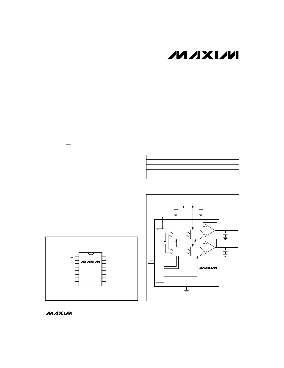
DAC
LATCH
A
DAC A
DAC
LATCH
B
DAC B
SCLK
OUTA
OUTB
DIN
REF
V
DD
CS
16-BIT SHIFT REGISTER
CONTROL (8)
DATA (8)
MAX522
8
3
1
5
6
7
2
0.1
µ
F
0.1
µ
F
(OPTIONAL)
0.01
µ
F
V
OUTA
V
OUTB
GND
4
0.22
µ
F
________________Functional Diagram
OUTB
V
DD
OUTA
GND
1
2
8
7
DIN
REF
SCLK
CS
MAX522
TOP VIEW
3
4
6
5
DIP/SO
__________________Pin Configuration
Call toll free 1-800-998-8800 for free samples or literature.
19-0403; Rev 0; 6/95
PART
TEMP. RANGE
PIN-PACKAGE
MAX522CPA
0°C to +70°C
8 Plastic DIP
MAX522CSA
0°C to +70°C
8 SO
MAX522EPA
-40°C to +85°C
8 Plastic DIP
SPI and QSPI are trademarks of Motorola Inc.
Microwire is a trademark of National Semiconductor Corp.
______________Ordering Information
MAX522ESA
-40°C to +85°C
8 SO
