Quad, serial 8-bit dacs with rail-to-rail outputs – Rainbow Electronics MAX510 User Manual
Page 16
MAX509/MAX510
where NB represents the digital input word. Since
AGND is common to all four DACs, all outputs will be
offset by V
BIAS
in the same manner. Do not bias AGND
more than +1V above DGND, or more than 2.5V below
DGND.
Figures 14 and 15 illustrate the generation of negative
offsets with bipolar outputs. In these circuits, AGND is
biased negatively (up to -2.5V with respect to DGND) to
provide an arbitrary negative output voltage for a 0
input code. The output voltage at OUTA is:
OUTA = -(R2/R1)(2.5V) + (NB/256)(2.5V)(R2/R1+1)
where NB represents the digital input word. Since
AGND is common to all four DACs, all outputs will be
offset by V
BIAS
in the same manner. Table 3, with
V
REF
= 2.5V, shows the digital code vs. output voltage
for Figure 14 and 15's circuits with R1 = R2. The
ICL7612 op amp is chosen because its common-mode
range extends to both supply rails.
Quad, Serial 8-Bit DACs
with Rail-to-Rail Outputs
16
______________________________________________________________________________________
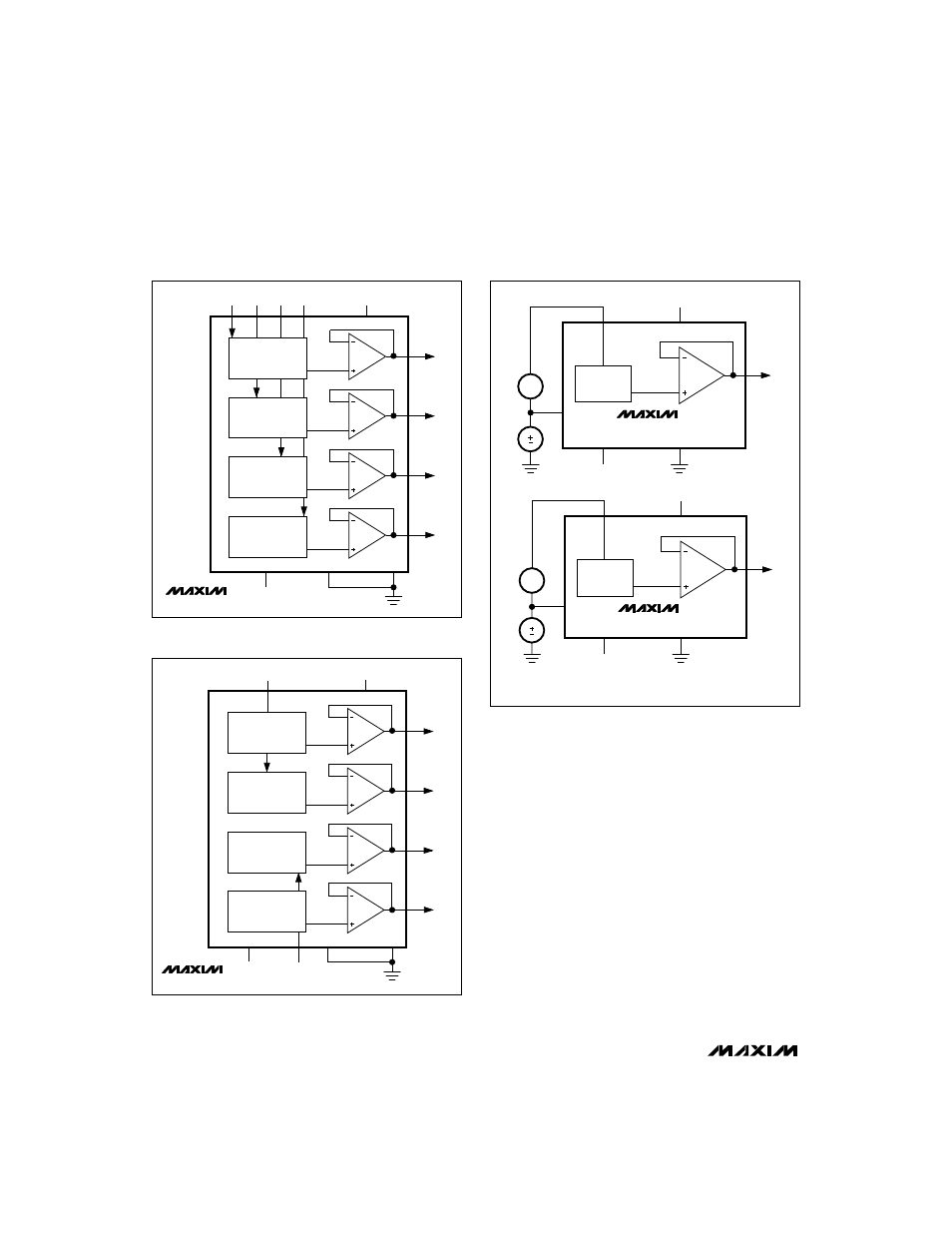
Figure 11. MAX509 Unipolar Output Circuit
REFD
DAC A
DAC B
DAC C
DAC D
REFC
REFB
REFA
MAX509
OUTA
OUTB
OUTC
OUTD
SERIAL
INTERFACE
NOT SHOWN
REFERENCE INPUTS (V
SS
TO V
DD
)
2
1
20
19
V
DD
+5V
16
5
17
4
18
3
-5V (OR GND)
6
8
V
SS
AGND
DGND
Figure 12. MAX510 Unipolar Output Circuit
DAC A
DAC B
DAC C
DAC D
REFAB
MAX510
OUTA
OUTB
OUTC
OUTD
SERIAL
INTERFACE
NOT SHOWN
REFERENCE INPUTS (V
SS
TO V
DD
)
2
1
16
15
V
DD
+5V
4
14
3
-5V (OR GND)
5
6
V
SS
AGND
DGND
REFCD
13
Figure 13. MAX509/MAX510 AGND Bias Circuits (Positive
Offset)
DAC A
MAX509
5
18
AGND
2
OUTA
DGND
V
SS
REFA
V
DD
3
8
V
IN
V
BIAS
6
+5V
-5V (OR GND)
DAC A
MAX510
4
14
AGND
2
OUTA
DGND
V
SS
REFAB
V
DD
3
6
V
IN
V
BIAS
5
+5V
-5V (OR GND)
SERIAL INTERFACE NOT SHOWN