Electrical characteristics (continued), Timing characteristics – Rainbow Electronics MAX510 User Manual
Page 4
MAX509/MAX510
Quad, Serial 8-Bit DACs
with Rail-to-Rail Outputs
4
_______________________________________________________________________________________
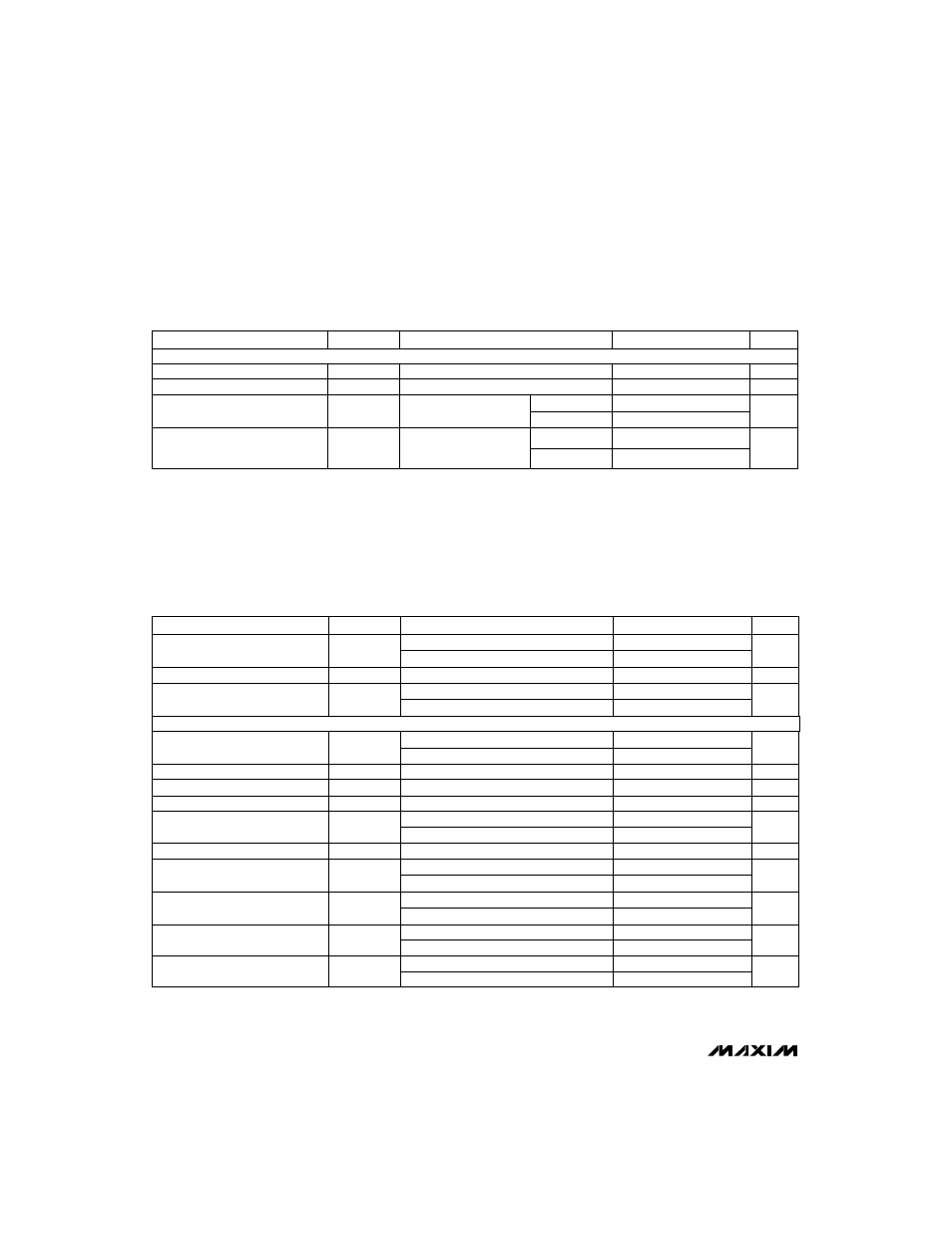
ELECTRICAL CHARACTERISTICS (continued)
(VDD = +5V ±10%, VSS = 0V to -5.5V, VREF = 4V, AGND = DGND = 0V, RL = 10k
Ω
, CL = 100pF, TA = TMIN to TMAX,
unless otherwise noted.)
PARAMETER
CONDITIONS
MIN
TYP
MAX
UNITS
Positive Supply Voltage
SYMBOL
4.5
5.5
V
For specified performance
V
DD
Negative Supply Voltage
-5.5
0
V
For specified performance
V
SS
5
10
Positive Supply Current
5
12
mA
I
DD
Negative Supply Current
mA
I
SS
5
10
MAX5_ _C/E
MAX5_ _M
MAX5_ _C/E
5
12
MAX5_ _M
V
SS
= -5V ±10%, outputs
unloaded, all digital
inputs = 0V or V
DD
Note 1:
Input resistance is code dependent. The lowest input resistance occurs at code = 55 hex.
Note 2:
Input capacitance is code dependent. The highest input capacitance occurs at code = 00 hex.
Note 3:
VREF = 4V
p-p
, 10kHz. Channel-to-channel isolation is measured by setting the code of one DAC to FF hex and setting the
code of all other DACs to 00 hex.
Note 4:
VREF = 4V
p-p
, 10kHz. DAC code = 00 hex.
Note 5:
Guaranteed by design.
Note 6:
Output settling time is measured by taking the code from 00 hex to FF hex, and from FF hex to 00 hex.
TIMING CHARACTERISTICS
(VDD = +5V ±10%, VSS = 0V to -5V, VREF = 4V, AGND = DGND = 0V, CL = 50pF, TA = TMIN to TMAX, unless otherwise noted.)
PARAMETER
CONDITIONS
MIN
TYP
MAX
UNITS
CLR Pulse Width Low
SYMBOL
50
25
ns
MAX5_ _M
MAX5_ _C/E
40
20
t
CLW
MAX5_ _M
50
25
ns
MAX5_ _C/E
40
20
SCLK Fall to
CS Rise Hold Time
0
ns
t
CSH2
SCLK Fall to
CS Fall Hold Time
0
ns
(Note 7)
t
CSH0
40
MAX5_ _C/E
10
100
MAX5_ _C/E
MAX5_ _C/E
40
40
MAX5_ _C/E
20
12.5
MAX5_ _C/E
DIN to SCLK Rise Hold Time
0
ns
t
DH
SCLK Rise to
CS Rise Hold Time
(Note 9)
40
ns
t
CSH1
LDAC Pulse Width Low
(Notes 7, 8)
0
ns
t
LDW
t
CLL
CS Rise to LDAC Fall Setup Time
40
MAX5_ _C/E
CS Fall to SCLK Setup Time
50
ns
MAX5_ _M
t
CSS
DIN to SCLK Rise Setup Time
50
ns
MAX5_ _M
t
DS
SCLK Clock Frequency
20
10
MHz
MAX5_ _M
f
CLK
SCLK Pulse Width High
50
ns
MAX5_ _M
t
CH
SCLK Pulse Width Low
MAX5_ _M
50
ns
t
CL
SCLK to DOUT Valid
10
100
ns
MAX5_ _M
t
DO
Note 7:
Guaranteed by design.
Note 8:
If
LDAC is activated prior to CS's rising edge, it must stay low for t
LDW
or longer after
CS goes high.
Note 9:
Minimum delay from 12th clock cycle to
CS rise.
Outputs unloaded, all
digital inputs = 0V or V
DD
POWER SUPPLIES
SERIAL INTERFACE TIMING