Electrical characteristics, Absolute maximum ratings – Rainbow Electronics MAX510 User Manual
Page 2
MAX509/MAX510
Quad, Serial 8-Bit DACs
with Rail-to-Rail Outputs
2
_______________________________________________________________________________________
V
DD
to DGND ..............................................................-0.3V, +6V
V
DD
to AGND...............................................................-0.3V, +6V
V
SS
to DGND ...............................................................-6V, +0.3V
V
SS
to AGND ...............................................................-6V, +0.3V
V
DD
to V
SS
.................................................................-0.3V, +12V
Digital Input Voltage to DGND ......................-0.3V, (V
DD
+ 0.3V)
REF_....................................................(V
SS
- 0.3V), (V
DD
+ 0.3V)
OUT_..............................................................................V
DD
, V
SS
Maximum Current into Any Pin............................................50mA
Continuous Power Dissipation (T
A
= +70°C)
16-Pin Plastic DIP (derate 10.53mW/°C above +70°C) ....842mW
16-Pin Wide SO (derate 9.52mW/°C above +70°C) .........762mW
16-Pin CERDIP (derate 10.00mW/°C above +70°C) ........800mW
20-Pin Plastic DIP (derate 11.11mW/°C above +70°C)....889mW
20-Pin Wide SO (derate 10.00mW/°C above +70°C) .......800mW
20-Pin SSOP (derate 10.00mW/°C above +70°C) ............800mW
20-Pin CERDIP (derate 11.11mW/°C above +70°C) ........889mW
Operating Temperature Ranges:
MAX5_ _ _C_ _ .....................................................0°C to +70°C
MAX5_ _ _E_ _ ..................................................-40°C to +85°C
MAX5_ _ _MJ_ ................................................-55°C to +125°C
Storage Temperature Range .............................-65°C to +150°C
Lead Temperature (soldering, 10sec) .............................+300°C
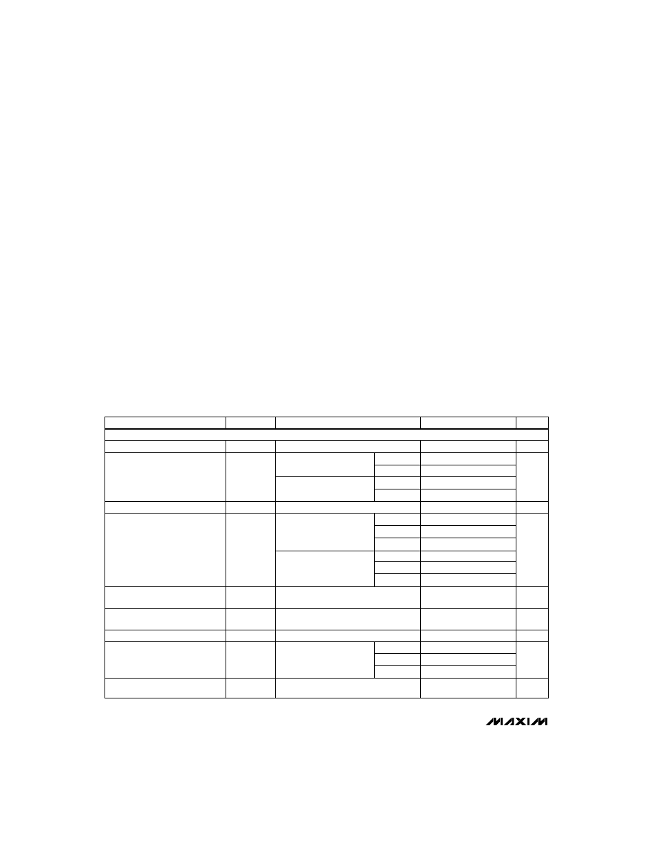
ELECTRICAL CHARACTERISTICS
(VDD = +5V ±10%, VSS = 0V to -5.5V, VREF = 4V, AGND = DGND = 0V, RL = 10k
Ω
, CL = 100pF, TA = TMIN to TMAX,
unless otherwise noted.)
Stresses beyond those listed under “Absolute Maximum Ratings” may cause permanent damage to the device. These are stress ratings only, and functional
operation of the device at these or any other conditions beyond those indicated in the operational sections of the specifications is not implied. Exposure to
absolute maximum rating conditions for extended periods may affect device reliability.
PARAMETER
CONDITIONS
MIN
TYP
MAX
UNITS
Note:
The outputs may be shorted to VDD, VSS, or AGND if the package power dissipation is not exceeded. Typical short-circuitcurrent
to AGND is 50mA. Do not bias AGND more than +1V above DGND, or more than 2.5V below DGND.
ABSOLUTE MAXIMUM RATINGS
Resolution
8
Bits
±1
MAX5_ _A
VREF = +4V,
VSS = 0V or -5V ±10%
MAX5_ _B
±1
MAX5_ _A
Total Unadjusted Error
VREF = -4V,
VSS = -5V ±10%
±1.5
LSB
Differential Nonlinearity
±1
LSB
Guaranteed monotonic
14
MAX5_ _C
16
MAX5_ _E
MAX5_ _B
±10
µV/°C
Code = FF hex
1
4
MAX5_ _C
Full-Scale Error
±14
mV
Code = FF hex
±10
µV/°C
Code = 00 hex
Zero-Code-Error Supply Rejection
1
2
mV
Code = 00 hex,
VSS = 0V
20
MAX5_ _M
SYMBOL
TUE
DNL
±14
MAX5_ _C
±16
MAX5_ _E
Zero-Code Error
Code = 00 hex,
VSS = -5V ±10%
±20
mV
MAX5_ _M
ZCE
±1.5
Code = 00 hex, V
DD
= 5V ±10%,
V
SS
= 0V or -5V ±10%
Zero-Code
Temperature Coefficient
1
8
MAX5_ _E
Full-Scale-Error Supply Rejection
Code = FF hex,
V
DD
= +5V ±10%,
V
SS
= 0V or -5V ±10%
1
12
mV
MAX5_ _M
Full-Scale-Error
Temperature Coefficient
STATIC ACCURACY