Quad, serial 8-bit dacs with rail-to-rail outputs – Rainbow Electronics MAX510 User Manual
Page 12
Set DOUT Phase – SCLK Falling (Mode 0)
This command resets DOUT to transition at SCLK's falling
edge. Once this command is issued, the phase of DOUT is
latched and will not change except on power-up or if the
specific command is issued that sets the phase to rising
edge.
The same command also updates all DAC registers with
the contents of their respective input registers, identical to
the “
LDAC” command.
LDAC Operation (Hardware)
LDAC is typically used in 4-wire interfaces (Figure 7).
LDAC allows asynchronous hardware control of the DAC
outputs and is level-sensitive. With
LDAC low, the DAC reg-
isters are transparent and any time an input register is
updated, the DAC output immediately follows.
Clear DACs with CLR
Strobing the
CLR pin low causes an asynchronous clear of
input and DAC registers and sets all DAC outputs to zero.
Similar to the
LDAC pin, CLR can be invoked at any time,
typically when the device is not selected (
CS = H). When
the DAC data is all zeros, this function is equivalent to the
"Update all DACs from Shift Registers" command.
Digital Inputs and Outputs
Digital inputs and outputs are compatible with both TTL and
5V CMOS logic. The power-supply current (I
DD
) depends
on the input logic levels. Using CMOS logic to drive
CS,
SCLK, DIN,
CLR and LDAC turns off the internal level trans-
lators and minimizes supply currents.
Serial Data Output
DOUT is the output of the internal shift register. DOUT can be
programmed to clock out data on SCLK's falling edge (mode
0) or rising edge (mode 1). In mode 0, output data lags the
input data by 12.5 clock cycles, maintaining compatibility with
Microwire, SPI, and QSPI. In mode 1, output data lags the input
by 12 clock cycles. On power-up, DOUT defaults to mode 1
timing. DOUT never three-states; it always actively drives either
high or low and remains unchanged when
CS is high.
Interfacing to the Microprocessor
The MAX509/MAX510 are Microwire, SPI, and QSPI compati-
ble. For SPI and QSPI, clear the CPOL and CPHA configura-
tion bits (CPOL = CPHA = 0). The SPI/QSPI CPOL = CPHA
= 1 configuration can also be used if the DOUT output is
ignored.
The MAX509/MAX510 can interface with Intel's
80C5X/80C3X family in mode 0 if the SCLK clock polarity is
inverted. More universally, if a serial port is not available,
three lines from one of the parallel ports can be used for bit
manipulation.
Digital feedthrough at the voltage outputs is greatly mini-
mized by operating the serial clock only to update the regis-
ters. Also see the Clock Feedthrough photo in the
Typical
Operating Characteristics section. The clock idle state is low.
Daisy-Chaining Devices
Any number of MAX509/MAX510s can be daisy-chained by
connecting the DOUT pin of one device to the DIN pin of the
following device in the chain. The NOP instruction (Table 1)
allows data to be passed from DIN to DOUT without chang-
ing the input or DAC registers of the passing device. A three-
wire interface updates daisy-chained or individual
MAX509/MAX510s simultaneously by bringing
CS high.
Quad, Serial 8-Bit DACs
with Rail-to-Rail Outputs
12
______________________________________________________________________________________
SCLK
DIN
DOUT
CS
SK
SO
SI
I/0
MICROWIRE
PORT
MAX509
MAX510
THE DOUT-SI CONNECTION IS NOT REQUIRED FOR WRITING TO THE
MAX509/MAX510, BUT MAY BE USED FOR READ-BACK PURPOSES.
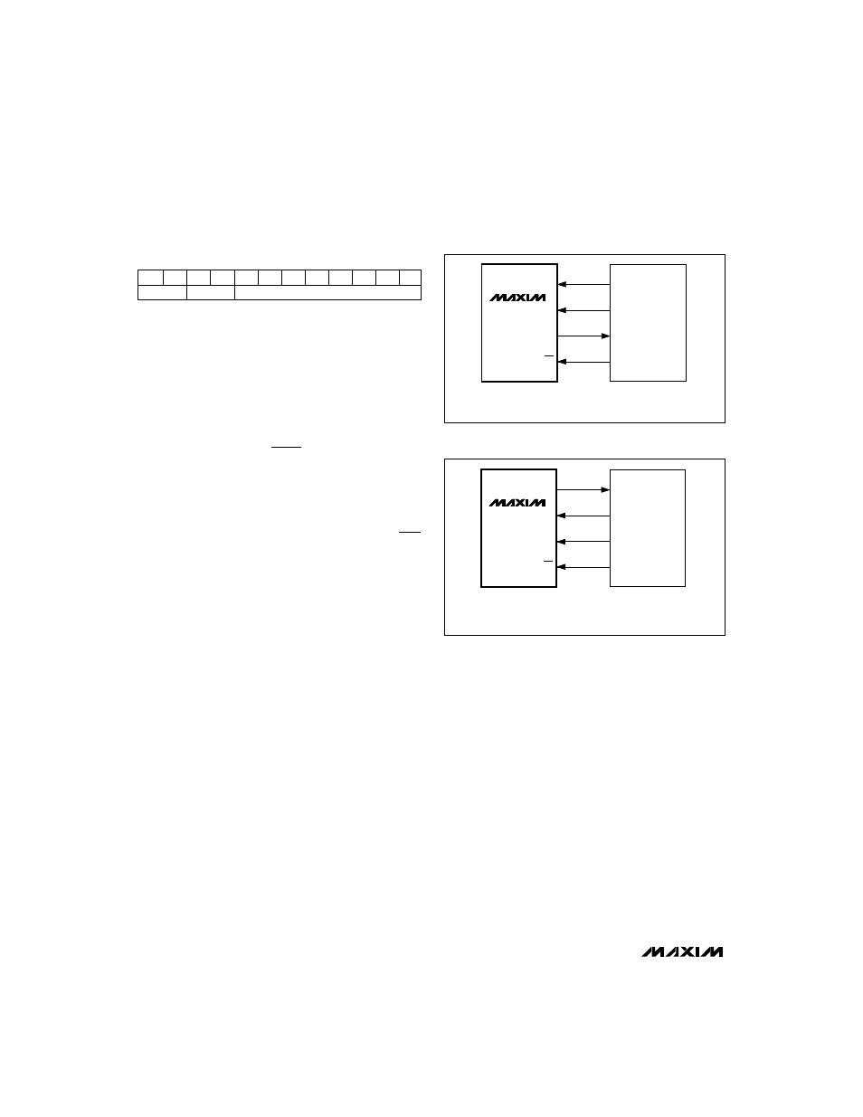
Figure 4. Connections for Microwire
DOUT
DIN
SCLK
CS
MISO
MOSI
SCK
I/0
SPI
PORT
MAX509
MAX510
THE DOUT-MISO CONNECTION IS NOT REQUIRED FOR WRITING TO THE
MAX509/MAX510, BUT MAY BE USED FOR READ-BACK PURPOSES.
CPOL = 0, CPHA = 0
Figure 5. Connections for SPI
(
LDAC = x)
A1
A0
C1
C0
D7
D6
D5
D4
D3
D2
D1
D0
x
x
x
x
x
x
x
x
1 0
1 0
MAX509/MAX510