Rainbow Electronics AT45DB321B User Manual
Megabit 2.7-volt only dataflash, Features, Description
1
Features
•
Single 2.7V - 3.6V Supply
•
Serial Peripheral Interface (SPI) Compatible
•
20 MHz Max Clock Frequency
•
Page Program Operation
– Single Cycle Reprogram (Erase and Program)
– 8192 Pages (528 Bytes/Page) Main Memory
•
Supports Page and Block Erase Operations
•
Two 528-byte SRAM Data Buffers – Allows Receiving of Data
while Reprogramming of Nonvolatile Memory
•
Continuous Read Capability through Entire Array
– Ideal for Code Shadowing Applications
•
Low Power Dissipation
– 4 mA Active Read Current Typical
– 2 µA CMOS Standby Current Typical
•
Hardware Data Protection Feature
•
100% Compatible to AT45DB321
•
5.0V-tolerant Inputs: SI, SCK, CS, RESET and WP Pins
•
Commercial and Industrial Temperature Ranges
Description
The AT45DB321B is a 2.7-volt only, serial interface Flash memory ideally suited for
a wide variety of digital voice-, image-, program code- and data-storage applications.
Its 34,603,008 bits of memory are organized as 8192 pages of 528 bytes each. In
ad d it io n t o t he m a in me m or y, t he AT45 DB3 21 B a l s o c o nt ains t wo S R A M
data buffers of 528 bytes each. The buffers allow receiving of data while a page in the
main memory is being reprogrammed, as well as reading or writing a continuous data
32-megabit
2.7-volt Only
DataFlash
®
AT45DB321B
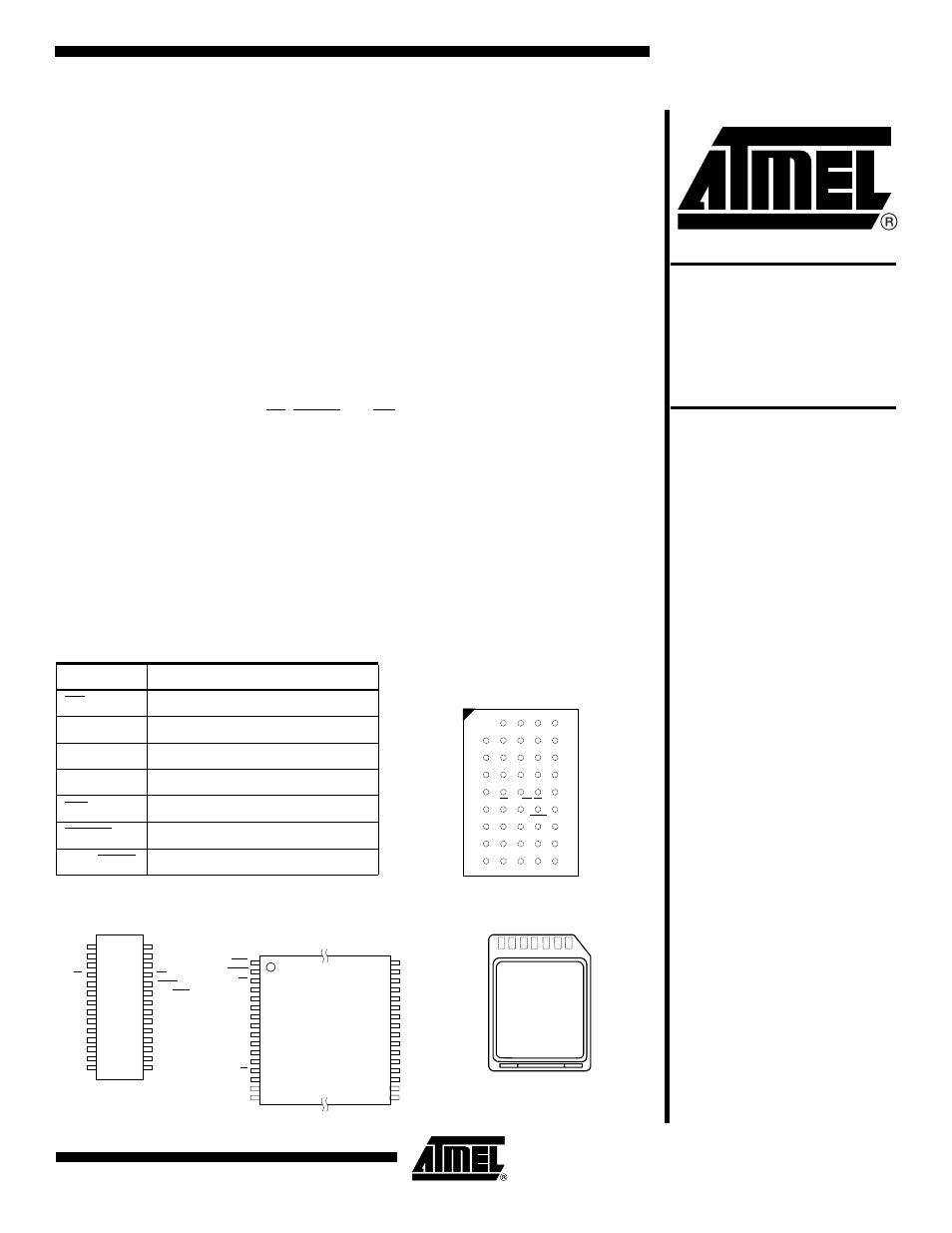
TSOP Top View
Type 1
1
2
3
4
5
6
7
8
9
10
11
12
13
14
15
16
RDY/BUSY
RESET
WP
NC
NC
NC
VCC
GND
NC
NC
NC
NC
CS
SCK
SI
SO
32
31
30
29
28
27
26
25
24
23
22
21
20
19
18
17
NC
NC
NC
NC
NC
NC
NC
NC
NC
NC
NC
NC
NC
NC
NC
NC
CBGA Top View through Package
A
B
C
D
E
F
G
H
J
1
2
3
4
5
NC
NC
NC
NC
NC
NC
NC
NC
NC
NC
NC
VCC
WP
RESET
NC
NC
NC
NC
NC
NC
GND
RDY/BSY
SI
NC
NC
NC
NC
NC
NC
SCK
CS
SO
NC
NC
NC
NC
NC
NC
NC
NC
NC
NC
NC
NC
Pin Configurations
Pin Name
Function
CS
Chip Select
SCK
Serial Clock
SI
Serial Input
SO
Serial Output
WP
Hardware Page Write Protect Pin
RESET
Chip Reset
RDY/BUSY
Ready/Busy
DataFlash Card
(1)
Note:
1.
See AT45DCB004 Datasheet
7 6 5 4 3 2 1
SOIC
1
2
3
4
5
6
7
8
9
10
11
12
13
14
28
27
26
25
24
23
22
21
20
19
18
17
16
15
GND
NC
NC
CS
SCK
SI
SO
NC
NC
NC
NC
NC
NC
NC
VCC
NC
NC
WP
RESET
RDY/BUSY
NC
NC
NC
NC
NC
NC
NC
NC
Rev. 2223D–DFLASH–10/02
Document Outline
- Features
- Description
- Block Diagram
- Memory Array
- Memory Architecture Diagram
- Device Operation
- Status Register Format
- Block Erase Addressing
- Power-on/Reset State
- Absolute Maximum Ratings*
- DC and AC Operating Range
- DC Characteristics
- AC Characteristics
- Input Test Waveforms and Measurement Levels
- Output Test Load
- AC Waveforms
- Write Operations
- Read Operations
- Detailed Bit-level Read Timing – Inactive Clock Polarity Low
- Detailed Bit-level Read Timing – Inactive Clock Polarity Low (Continued)
- Detailed Bit-level Read Timing – Inactive Clock Polarity High
- Detailed Bit-level Read Timing – Inactive Clock Polarity High (Continued)
- Detailed Bit-level Read Timing – SPI Mode 0
- Detailed Bit-level Read Timing – SPI Mode 0 (Continued)
- Detailed Bit-level Read Timing – SPI Mode 3
- Detailed Bit-level Read Timing – SPI Mode 3 (Continued)
- Sector Addressing
- Ordering Information
- Packaging Information