Typical operating characteristics – Rainbow Electronics DS1859 User Manual
Page 5
DS1859
Dual, Temperature-Controlled Resistors with
Internally Calibrated Monitors
_____________________________________________________________________
5
Note 10: After this period, the first clock pulse is generated.
Note 11: The maximum t
HD:DAT
only has to be met if the device does not stretch the LOW period (t
LOW
) of the SCL signal.
Note 12: A device must internally provide a hold time of at least 300ns for the SDA signal (see the V
IH MIN
of the SCL signal) to
bridge the undefined region of the falling edge of SCL.
Note 13: C
B
—total capacitance of one bus line, timing referenced to 0.9 x V
CC
and 0.1 x V
CC
.
Note 14: Guaranteed by design.
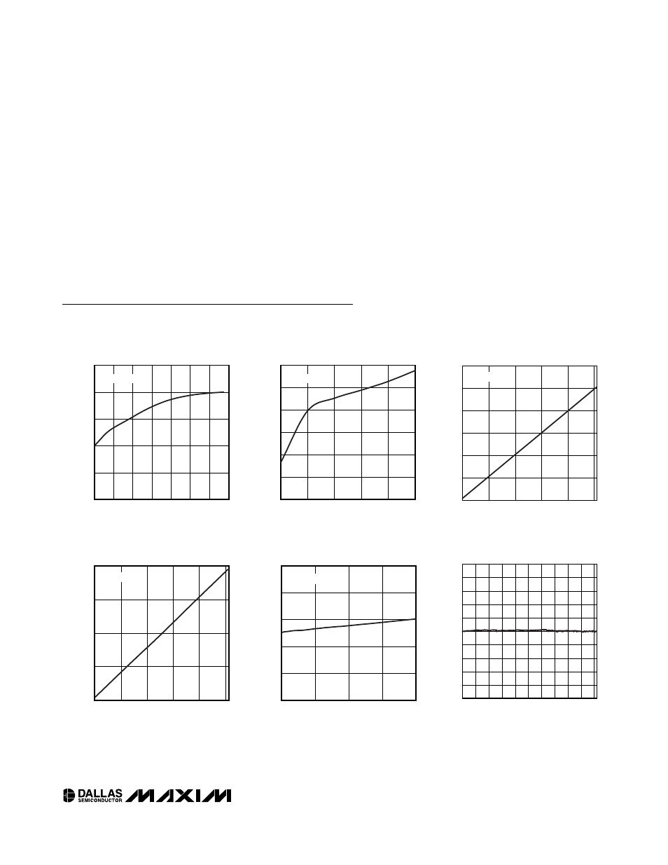
Typical Operating Characteristics
(V
CC
= 5.0V, T
A
= +25°C, for both 50k
Ω and 20kΩ versions, unless otherwise noted.)
TEMPERATURE (
°C)
40
60
80
20
0
-20
560
600
640
680
720
520
-40
100
SUPPLY CURRENT vs. TEMPERATURE
DS1859 toc01
SUPPLY CURRENT (
µ
A)
SDA = SCL = V
CC
SUPPLY CURRENT vs. VOLTAGE
DS1859 toc02
VOLTAGE (V)
SUPPLY CURRENT (
µ
A)
5.0
4.5
4.0
3.5
450
500
550
600
650
700
400
3.0
5.5
SDA = SCL = V
CC
RESISTANCE vs. SETTING
DS1859 toc03
SETTING (DEC)
RESISTANCE (k
Ω
)
200
150
100
50
10
20
30
40
50
60
0
0
250
50k
Ω VERSION
RESISTANCE vs. SETTING
DS1859 toc04
SETTING (DEC)
RESISTANCE (k
Ω
)
200
150
100
50
5
10
15
20
0
0
250
20k
Ω VERSION
ACTIVE SUPPLY CURRENT
vs. SCL FREQUENCY
DS1859 toc05
SCL FREQUENCY (kHz)
ACTIVE SUPPLY CURRENT (
µ
A)
300
200
100
600
640
680
720
760
560
0
400
SDA = V
CC
RESISTOR 0 INL (LSB)
DS1859 toc06
SETTING (DEC)
RESISTOR 0 INL (LSB)
225
200
150 175
50 75 100 125
25
-0.8
-0.6
-0.4
-0.2
0
0.2
0.4
0.6
0.8
1.0
-1.0
0
250