Table 8. calibration constants – Rainbow Electronics DS1859 User Manual
Page 22
DS1859
Dual, Temperature-Controlled Resistors with
Internally Calibrated Monitors
22
____________________________________________________________________
Programming the Look-up Table (LUT)
The following equation can be used to determine which
resistor position setting, 00h to FFh, should be written in
the LUT to achieve a given resistance at a specific tem-
perature.
α = 3.852357 for the 20kΩ resistor
α = 4.5680475 for the 50kΩ resistor
R = the resistance desired at the output terminal
C = temperature in degrees Celsius
u, v, w, x
1
, x
0
, y, and z are calculated values found in the
corresponding look-up tables. The variable x from the
equation above is separated into x
1
(the MSB of x) and x
0
(the LSB of x). Their addresses and LSB values are given
below. Resistor 0 variables are found in Table 1, and
Resistor 1 variables are found in Table 2.
When shipped from the factory, all other memory loca-
tions in the LUTs are programmed to FFh.
Table
8. Calibration Constants
Internal Calibration
The DS1859 has two methods for scaling an analog
input to a digital result. The two methods are gain and
offset. Each of the inputs (V
CC
, MON1, MON2, and
MON3) has a unique register for the gain and the offset
found in
Table
01h, 92h to 99h, and A2h to A9h.
To scale the gain and offset of the converter for a spe-
cific input, you must first know the relationship between
the analog input and the expected digital result. The
input that would produce a digital result of all zeros is
the null value (normally this input is GND). The input
that would produce a digital result of all ones is the full-
scale (FS) value. The FS value is also found by multiply-
ing an all-ones digital answer by the weighted LSB
(e.g., since the digital reading is a 16-bit register, let us
assume that the LSB of the lowest weighted bit is
50µV, then the FS value is 65,535 x 50µV = 3.27675V).
A binary search is used to scale the gain of the con-
verter. This requires forcing two known voltages to the
input pin. It is preferred that one of the forced voltages
is the null input and the other is 90% of FS. Since the
LSB of the least significant bit in the digital reading reg-
ister is known, the expected digital results are also
known for both inputs (null/LSB = CNT1 and 90%FS/
LSB = CNT2).
The user might not directly force a voltage on the input.
Instead they have a circuit that transforms light, fre-
quency, power, or current to a voltage that is the input
to the DS1859. In this situation, the user does not need
to know the relationship of voltage to expected digital
result but instead knows the relationship of light, fre-
quency, power, or current to the expected digital result.
pos
R C
R u
v
C
w
C
x
y
C
z
C
α,
α
,
•
•
•
•
•
•
(
)
=
−
+
−
(
)
+
−
(
)
⎡
⎣⎢
⎤
⎦⎥
( )
+
−
(
)
+
−
(
)
⎡
⎣⎢
⎤
⎦⎥
−
1
25
25
1
25
25
2
2
M6
M5
M4
M3
M2
M1
2
4
6
8
10
12
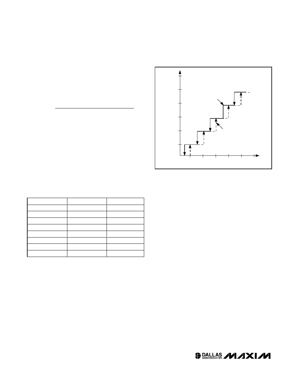
TEMPERATURE (
°C)
MEMORY LOCATION
INCREASING
TEMPERATURE
DECREASING
TEMPERATURE
Figure 4. Look-Up Table Hysteresis
ADDRESS (Hex)
VARIABLE
LSB
F8
u
2
0
F9
v
20E-6
FA
w
100-9
FB
x
1
2
1
FC
x
0
2
-7
FD
y
2E-6
FE
z
10E-9
FF
Reserved
—