Register map, Auxiliary device, Main device – Rainbow Electronics DS1859 User Manual
Page 13
DS1859
Dual, Temperature-Controlled Resistors with
Internally Calibrated Monitors
____________________________________________________________________
13
MEMORY LOCATION
(hex)
EEPROM/SRAM
R/W
DEFAULT SETTING
(hex)
NAME OF LOCATION
FUNCTION
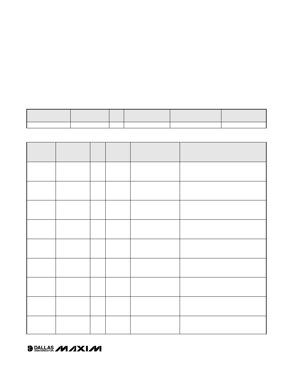
00 to 7F
EEPROM
R/W
00
Standards Data
—
Auxiliary Device
MEMORY
LOCATION
(hex)
EEPROM/
SRAM
R/W
DEFAULT
SETTING
(hex)
NAME OF LOCATION
FUNCTION
00 to 01
EEPROM
R/W
00
TMPlimhi (MSB to LSB)
Contains upper limit settings for temperature.
If the limit is violated, an alarm flag in Main
Device byte 70h is set.
02 to 03
EEPROM
R/W
00
TMPlimlo (MSB to LSB)
Contains lower limit settings for temperature. If
the limit is violated, an alarm flag in Main
Device byte 70h is set.
04 to 05
EEPROM
R/W
00
TMPwrnhi (MSB to LSB)
Contains upper limit settings for temperature.
If the limit is violated, a warning flag in Main
Device byte 74h is set.
06 to 07
EEPROM
R/W
00
TMPwrnlo (MSB to LSB)
Contains lower limit settings for temperature. If
the limit is violated, a warning flag in Main
Device byte 74h is set.
08 to 09
EEPROM
R/W
00
V
CC
limhi (MSB to LSB)
Contains upper limit settings for V
CC
. If the
limit is violated, an alarm flag in Main Device
byte 70h is set.
0A to 0B
EEPROM
R/W
00
V
CC
limlo (MSB to LSB)
Contains lower limit settings for V
CC
. If the
limit is violated, an alarm flag in Main Device
byte 70h is set.
0C to 0D
EEPROM
R/W
00
V
CC
wrnhi (MSB to LSB)
Contains upper limit settings for V
CC
. If the
limit is violated, a warning flag in Main Device
byte 74h is set.
0E to 0F
EEPROM
R/W
00
V
CC
wrnlo (MSB to LSB)
Contains lower limit settings for V
CC
. If the
limit is violated, a warning flag in Main Device
byte 74h is set.
10 to 11
EEPROM
R/W
00
MON1limhi (MSB to LSB)
Contains upper limit settings for MON1. If the
limit is violated, an alarm flag in Main Device
byte 70h is set.
Main Device
Note: SRAM defaults are power-on defaults. EEPROM defaults are factory defaults.
Register Map
A description of the registers is below. The registers
are read only (R) or read/write (R/W). The R/W registers
are writable only if write protect has not been asserted
(see the Memory Description section).
Bytes designated as "Reserved" have been set aside
for added functionality in future revisions of this device.