Table 4. aden address configuration, Table 5. aden and adfix bits – Rainbow Electronics DS1859 User Manual
Page 11
DS1859
Dual, Temperature-Controlled Resistors with
Internally Calibrated Monitors
____________________________________________________________________
11
Variable Resistors
The value of each variable resistor is determined by
a temperature-addressed look-up
table
, which can
assign a unique value (00h to FFh) to each resistor for
every 2°C increment over the -40°C to +102°C range
(see
Table
3). See the Temperature Conversion section
for more information.
The variable resistors can also be used in manual
mode. If the TEN bit equals 0, the resistors are in manu-
al mode and the temperature indexing is disabled. The
user sets the resistors in manual mode by writing to
addresses 82h and 83h in Table 01 to control resistors
0 and 1, respectively.
Memory Description
Main and auxiliary memories can be accessed by two
separate device addresses. The Main Device address
is A2h (or value in Table 01 byte 8Ch, when ADFIX = 1)
and the Auxiliary Device address is A0h. A user option
is provided to respond to one or two device addresses.
This feature can be used to save component count in
SFF applications (Main Device address can be used)
or other applications where both GBIC (Auxiliary
Device address can be used) and monitoring functions
are implemented and two device addresses are need-
ed. The memory blocks are enabled with the corre-
sponding device address. Memory space from 80h and
ADEN
(ADDRESS
ENABLE)
NO. OF SEPARATE
DEVICE
ADDRESSES
ADDITIONAL
INFORMATION
0
2
See Figure 2
1
1 (Main Device only)
See Figure 3
Table 4. ADEN Address Configuration
ADEN
ADFIX
AUXILIARY
ADDRESS
MAIN ADDRESS
0
0
A0h
A2h
0
1
A0h
EEPROM
(Table 01, 8Ch)
1
0
N/A
A2h
1
1
N/A
EEPROM
(Table 01, 8Ch)
Table 5. ADEN and ADFIX Bits
MAIN
DEVICE
MON LOOK-UP
TABLE CONTROL
R0 LOOK-UP
TABLE
AUXILIARY
DEVICE
0
DEC
0
95
96
127
128
143
199
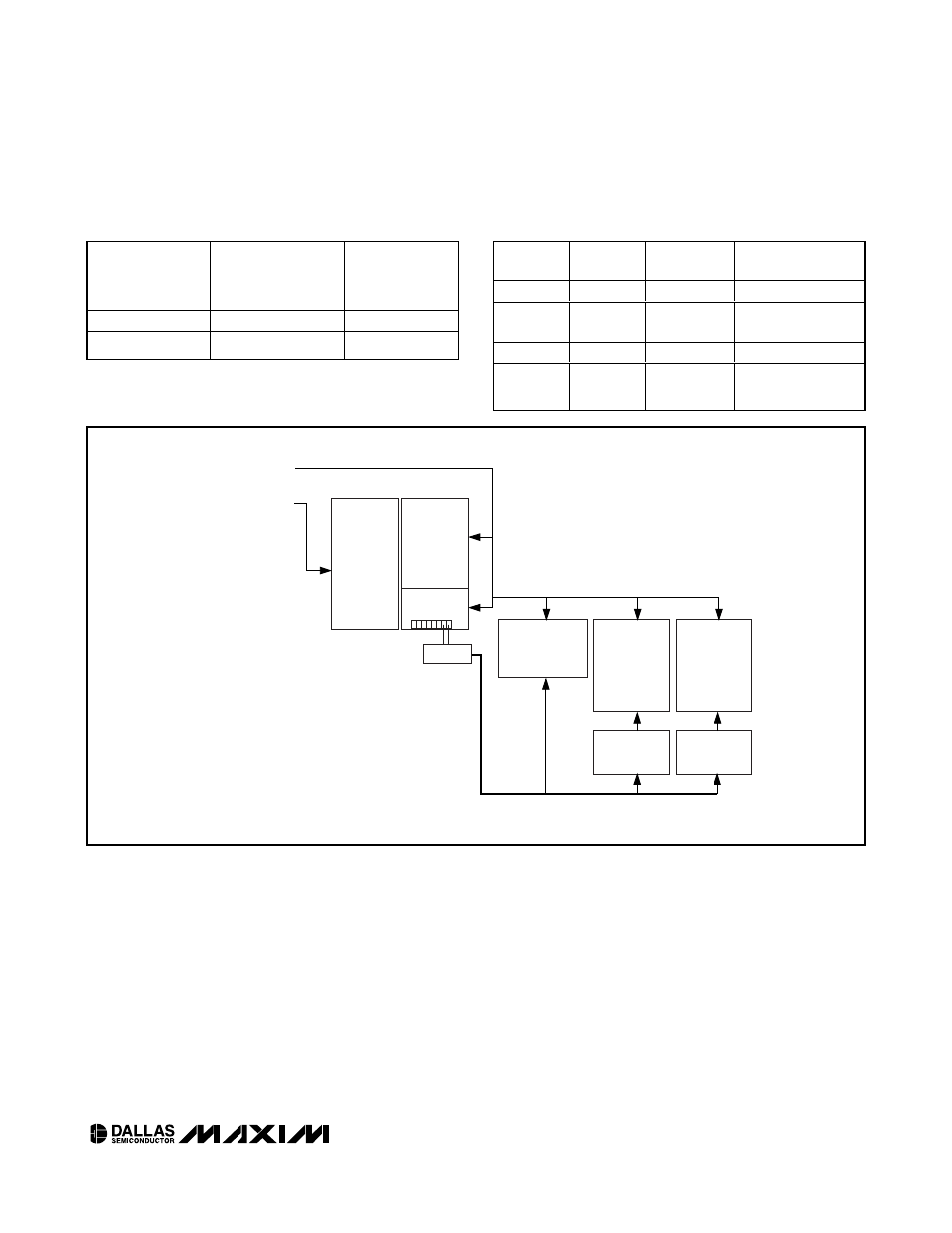
MEMORY PARTITION WITH ADEN BIT = 0
EN
EN
EN
5Fh
60h
EN
SEL
EN
SEL
7Fh
7Fh
80h
80h
C7h
F0h
FFh
RESERVED
8Fh
TABLE SELECT
MAIN DEVICE ENABLE
AUXILIARY DEVICE ENABLE
DECODER
0
F0h
FFh
RESERVED
R1 LOOK-UP
TABLE
EN
SEL
80h
C7h
TABLE 03
TABLE 02
TABLE 01
Figure 2. Memory Organization, ADEN = 0