Main device (continued) – Rainbow Electronics DS1859 User Manual
Page 15
DS1859
Dual, Temperature-Controlled Resistors with
Internally Calibrated Monitors
____________________________________________________________________
15
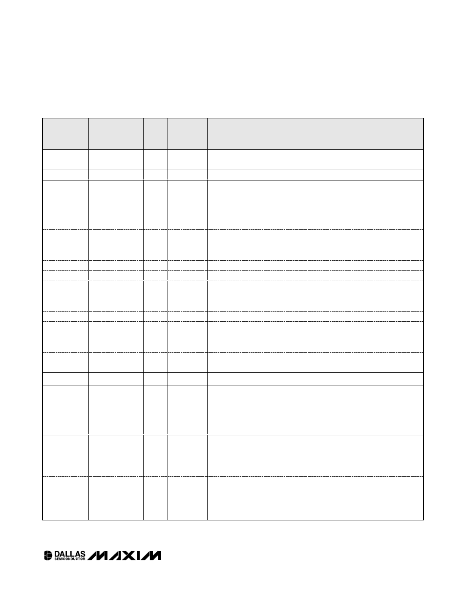
MEMORY
LOCATION
(hex)
EEPROM/
SRAM
R/W
DEFAULT
SETTING
(hex)
NAME OF LOCATION
FUNCTION
68 to 69
SRAM
R
—
Measured MON3
(MSB to LSB)
Digitized measured value for MON3.
See Table 1.
6A to 6D
SRAM
—
—
Reserved
—
6E
SRAM
—
—
Logic states
—
Bit 7
—
R
X
HIZSTA
Resistor status bit. A high indicates that both
resistors are in high-impedance mode. A low
indicates that both resistors are operating
normally.
6
—
R/W
0
HIZCO
Resistor control bit. Setting this bit high
causes both resistors to go into a high-
impedance state.
5
—
—
X
X
—
4
—
—
X
X
—
2
—
R
X
TXF
This status bit is high when OUT1 is high,
assuming there is an external pullup resistor
on OUT1.
3
—
—
X
X
—
1
—
R
X
RXL
This status bit is high when OUT2 is high,
assuming there is an external pullup resistor
on OUT2.
0
—
R
X
RDYB
This status bit goes high when V
CC
has fallen
below the POA level.
6F
SRAM
—
—
Conversion updates
—
Bit 7
—
R/W
0
TAU
This bit goes high after a temperature and
address update has occurred for the
corresponding measurement in bytes 60h to
61h. This bit can be written to a 0 by the user
and monitored to verify that a conversion has
occurred.
6
—
R/W
0
V
CC
U
This bit goes high after a V
CC
update has
occurred for the corresponding measurement
in bytes 62h to 63h. This bit can be written to
a 0 by the user and monitored to verify that a
conversion has occurred.
5
—
R/W
0
MON1U
This bit goes high after a MON1 update has
occurred for the corresponding measurement
in bytes 64h to 65h. This bit can be written to
a 0 by the user and monitored to verify that a
conversion has occurred.
Main Device (continued)