Rainbow Electronics DS1859 User Manual
Page 25
DS1859
Dual, Temperature-Controlled Resistors with
Internally Calibrated Monitors
____________________________________________________________________
25
Write Operations
After receiving a matching address byte with the R/W
bit set low, if there is no write protect, the device goes
into the write mode of operation (see the Memory
Organization section). The master must transmit an 8-
bit EEPROM memory address to the device to define
the address where the data is to be written. After the
byte has been received, the DS1859 transmits a zero
for one clock cycle to acknowledge the address has
been received. The master must then transmit an 8-bit
data word to be written into this address. The DS1859
again transmits a zero for one clock cycle to acknowl-
edge the receipt of the data. At this point, the master
must terminate the write operation with a STOP condi-
tion. The DS1859 then enters an internally timed write
process t
w
to the EEPROM memory. All inputs are dis-
abled during this byte write cycle.
Page Write
The DS1859 is capable of an 8-byte page write. A page
is any 8-byte block of memory starting with an address
evenly divisible by eight and ending with the starting
address plus seven. For example, addresses 00h
through 07h constitute one page. Other pages would
be addresses 08h through 0Fh, 10h through 17h, 18h
through 1Fh, etc.
A page write is initiated the same way as a byte write,
but the master does not send a STOP condition after
the first byte. Instead, after the slave acknowledges the
data byte has been received, the master can send up
to seven more bytes using the same nine-clock
sequence. The master must terminate the write cycle
with a STOP condition or the data clocked into the
DS1859 will not be latched into permanent memory.
The address counter rolls on a page during a write. The
counter does not count through the entire address
space as during a read. For example, if the starting
address is 06h and 4 bytes are written, the first byte
goes into address 06h. The second goes into address
07h. The third goes into address 00h (not 08h). The
fourth goes into address 01h. If more than 9 bytes or
more are written before a STOP condition is sent, the
first bytes sent are overwritten. Only the last 8 bytes of
data are written to the page.
Acknowledge Polling: Once the internally timed write
has started and the DS1859 inputs are disabled,
acknowledge polling can be initiated. The process
involves transmitting a START condition followed by the
device address. The R/W bit signifies the type of opera-
tion that is desired. The read or write sequence will only
be allowed to proceed if the internal write cycle has
completed and the DS1859 responds with a zero.
Read Operations
After receiving a matching address byte with the R/W bit
set high, the device goes into the read mode of opera-
tion. There are three read operations: current address
read, random read, and sequential address read.
Current Address Read
The DS1859 has an internal address register that main-
tains the address used during the last read or write
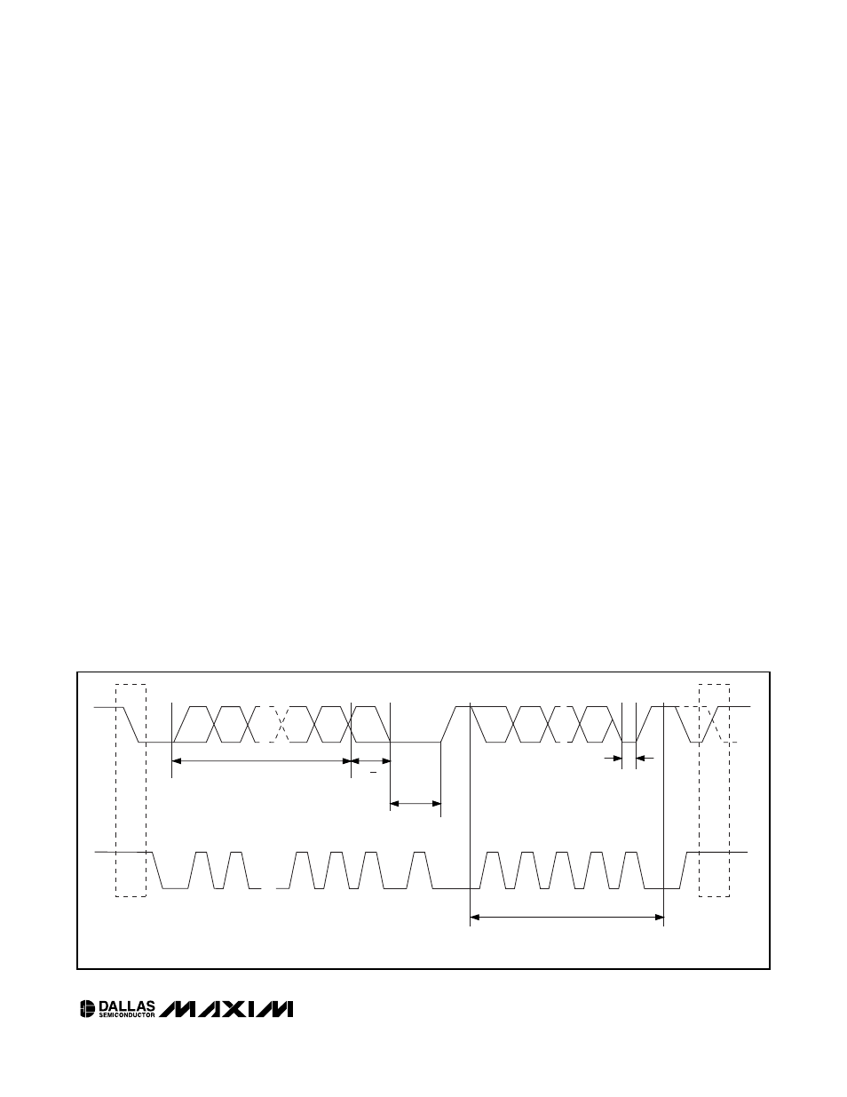
STOP
CONDITION
OR REPEATED
START
CONDITION
REPEATED IF MORE BYTES
ARE TRANSFERRED
ACK
START
CONDITION
ACK
ACKNOWLEDGEMENT
SIGNAL FROM RECEIVER
ACKNOWLEDGEMENT
SIGNAL FROM RECEIVER
SLAVE ADDRESS
MSB
SCL
SDA
R/W
DIRECTION
BIT
1
2
6
7
8
9
1
2
8
9
3–7
Figure 5. 2-Wire Data Transfer Protocol