Block diagram, Device description, Block diagram device description – Rainbow Electronics AT17F080 User Manual
Page 4
4
AT17F040/080
3039C–CNFG–11/02
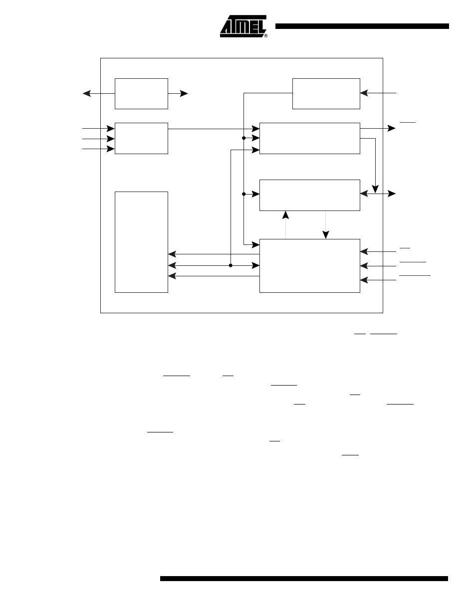
Block Diagram
Device Description
The control signals for the configuration memory device (CE, RESET/OE and CLK)
interface directly with the FPGA device control signals. All FPGA devices can control the
entire configuration process and retrieve data from the configuration device without
requiring an external intelligent controller.
The RESET/OE and CE pins control the tri-state buffer on the DATA output pin and
enable the address counter. When RESET/OE is driven Low, the configuration device
resets its address counter and tri-states its DATA pin. The CE pin also controls the out-
put of the AT17F Series Configurator. If CE is held High after the RESET/OE reset
pulse, the counter is disabled and the DATA output pin is tri-stated. When OE is subse-
quently driven High, the counter and the DATA output pin are enabled. When
RESET/OE is driven Low again, the address counter is reset and the DATA output pin is
tri-stated, regardless of the state of CE.
When the configurator has driven out all of its data and CEO is driven Low, the device
tri-states the DATA pin to avoid contention with other configurators. Upon power-up, the
address counter is automatically reset.
Config. Page
Select
Power-on
Reset
Flash
Memory
Clock/Oscillator
Logic
2-wire Serial Programming
Serial Download Logic
Control Logic
CLK
CEO(A2)
DATA
CE
RESET/OE
SER_EN
CE/WE/OE
Data
Address
READY
PAGE_EN
PAGESEL0
PAGESEL1
Reset