Block diagram – Rainbow Electronics AT49F001NT User Manual
Page 2

AT49F001(N)(T)
2
When the device is deselected, the CMOS standby current
is less than 100
µ
A. For the AT49F001N(T) pin 1 for the
DIP and PLCC packages and pin 9 for the TSOP package
are don’t connect pins.
To allow for simple in-system reprogrammability, the
AT49F001(N)(T) does not require high input voltages for
programming. Five-volt-only commands determine the read
and programming operation of the device. Reading data
out of the device is similar to reading from an EPROM; it
has standard CE, OE, and WE inputs to avoid bus conten-
tion. Reprogramming the AT49F001(N)(T) is performed by
erasing a block of data and then programming on a byte-
by-byte basis. The byte programming time is a fast 50 µs.
The end of a program cycle can be optionally detected by
the DATA polling feature. Once the end of a byte program
cycle has been detected, a new access for a read or pro-
gram can begin. The typical number of program and erase
cycles is in excess of 10,000 cycles.
The device is erased by executing the erase command
sequence; the device internally controls the erase opera-
tions. There are two 8K byte parameter block sections and
two main memory blocks.
The device has the capability to protect the data in the boot
block; this feature is enabled by a command sequence.
The 16K-byte boot block section includes a reprogramming
lock out feature to provide data integrity. The boot sector is
designed to contain user secure code, and when the fea-
ture is enabled, the boot sector is protected from being
reprogrammed.
In the AT49F001(N)(T), once the boot block programming
lockout feature is enabled, the contents of the boot block
a r e p e r m a n e n t a n d c a n n o t b e c h a n g e d . I n t h e
AT49F001(T), once the boot block programming lockout
feature is enabled, the contents of the boot block cannot be
changed with input voltage levels of 5.5 volts or less.
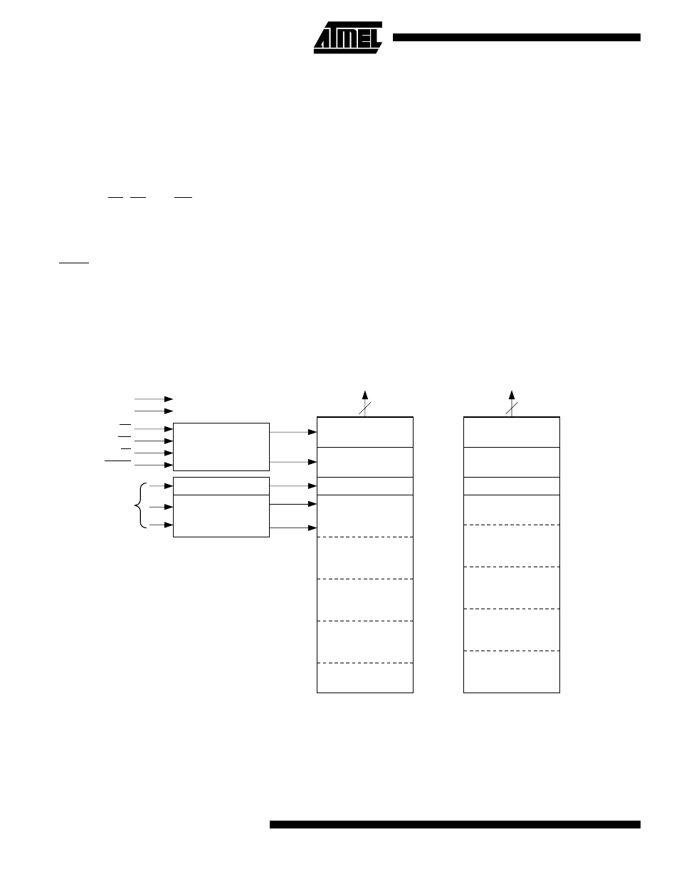
Block Diagram
CONTROL
LOGIC
Y DECODER
PARAMETER
BLOCK 1
(8K BYTES)
BOOT BLOCK
(16K BYTES)
OE
WE
CE
RESET
ADDRESS
INPUTS
VCC
GND
AT49F001(N)T
DATA INPUTS/OUTPUTS
I/O7 - I/O0
8
X DECODER
PARAMETER
BLOCK 2
(8K BYTES)
MAIN MEMORY
BLOCK 1
(32K BYTES)
MAIN MEMORY
BLOCK 2
(64K BYTES)
PROGRAM
DATA LATCHES
Y-GATING
INPUT/OUTPUT
BUFFERS
1FFFF
1C000
1BFFF
1A000
19FFF
18000
17FFF
10000
0FFFF
00000
PARAMETER
BLOCK 1
(8K BYTES)
BOOT BLOCK
(16K BYTES)
AT49F001(N)
DATA INPUTS/OUTPUTS
I/O7 - I/O0
8
PARAMETER
BLOCK 2
(8K BYTES)
MAIN MEMORY
BLOCK 1
(32K BYTES)
MAIN MEMORY
BLOCK 2
(64K BYTES)
PROGRAM
DATA LATCHES
Y-GATING
INPUT/OUTPUT
BUFFERS
1FFFF
10000
0FFFF
08000
07FFF
06000
05FFF
04000
03FFF
00000
