System considerations, Block diagram – Rainbow Electronics AT27LV256A User Manual
Page 2
AT27LV256A
2
making it ideal for fast, portable systems using battery
power.
Atmel’s innovative design techniques provide fast speeds
that rival 5V parts while keeping the low power consump-
tion of a 3.3V supply. At V
CC
= 3.0V, any byte can be
accessed in less than 55 ns. With a typical power dissipa-
t i on o f o n l y 1 8 m W a t 5 MH z a n d V
C C
= 3 .3 V , t h e
AT27LV256A consumes less than one fifth the power of a
standard 5V EPROM.
Standby mode supply current is typically less than 1
µA at
3.3V.
The AT27LV256A is available in industry standard JEDEC-
approved one-time programmable (OTP) plastic PLCC,
SOIC and TSOP packages. All devices feature two-line
control (CE, OE) to give designers the flexibility to prevent
bus contention.
The AT27LV256A operating with V
CC
at 3.0V produces TTL
level outputs that are compatible with standard TTL logic
devices operating at V
CC
= 5.0V. The device is also capa-
ble of standard 5-volt operation making it ideally suited for
dual supply range systems or card products that are plug-
gable in both 3-volt and 5-volt hosts.
Atmel’s AT27LV256A has additional features to ensure
high quality and efficient production use. The Rapid™ Pro-
gramming Algorithm reduces the time required to program
the part and guarantees reliable programming. Program-
ming time is typically only 100
µs/byte. The Integrated
Product Identification Code electronically identifies the
device and manufacturer. This feature is used by industry
standard programming equipment to select the proper pro-
gramming algorithms and voltages. The AT27LV256A pro-
grams exactly the same way as a standard 5V AT27C256R
and uses the same programming equipment.
System Considerations
Switching between active and standby conditions via the
Chip Enable pin may produce transient voltage excursions.
Unless accommodated by the system design, these tran-
sients may exceed data sheet limits, resulting in device
non-conformance. At a minimum, a 0.1
µF high frequency,
low inherent inductance, ceramic capacitor should be uti-
lized for each device. This capacitor should be connected
between the V
CC
and Ground terminals of the device, as
close to the device as possible. Additionally, to stabilize the
supply voltage level on printed circuit boards with large
EPROM arrays, a 4.7
µF bulk electrolytic capacitor should
be utilized, again connected between the V
CC
and Ground
terminals. This capacitor should be positioned as close as
possible to the point where the power supply is connected
to the array.
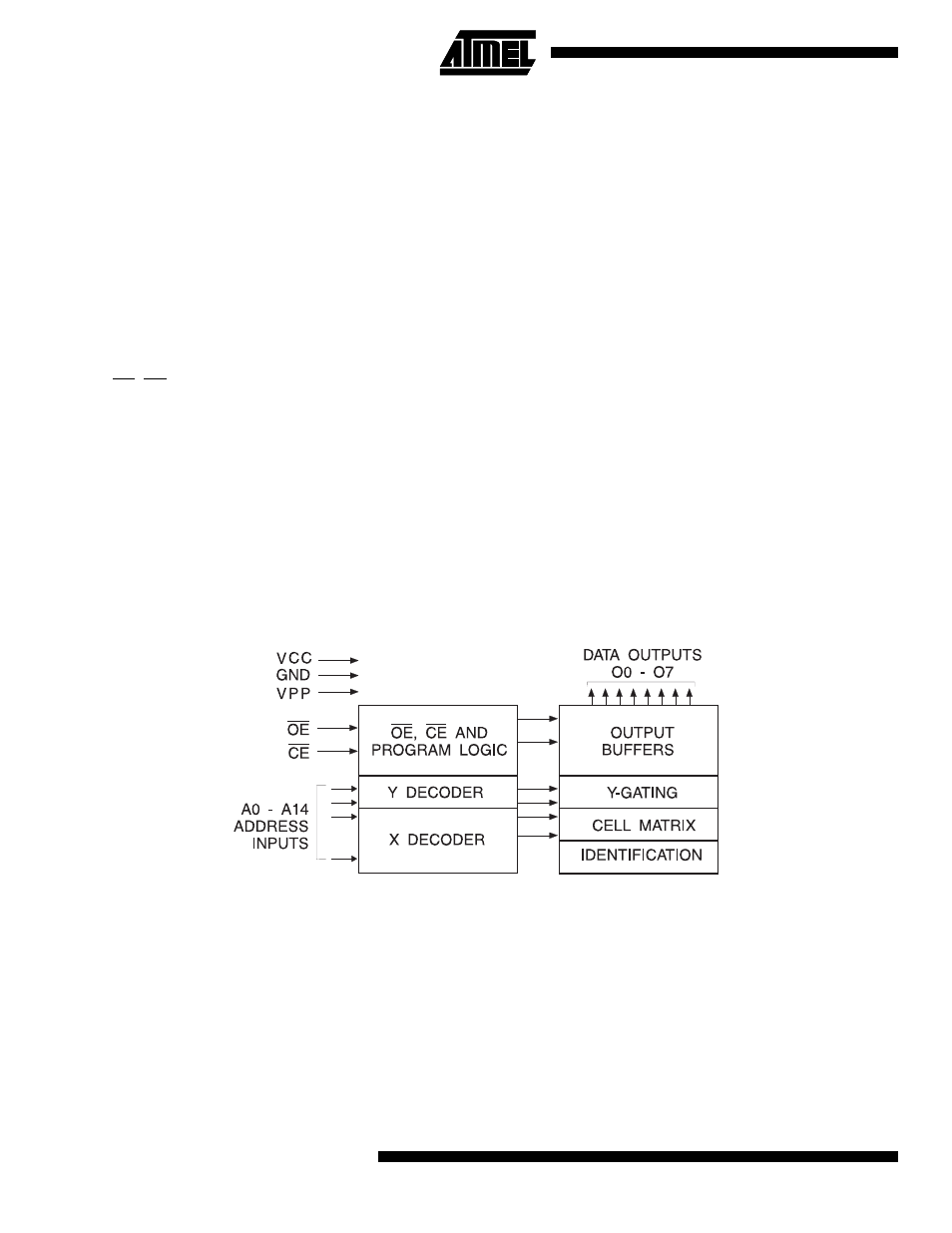
Block Diagram