Block diagram, Device operation, Block diagram device operation – Rainbow Electronics AT29C040A User Manual
Page 2
2
AT29C040A
0333I–FLASH–05/02
To allow for simple in-system reprogrammability, the AT29C040A does not require high input
voltages for programming. Five-volt-only commands determine the operation of the device.
Reading data out of the device is similar to reading from an EPROM. Reprogramming the
AT29C040A is performed on a sector basis; 256 bytes of data are loaded into the device and
then simultaneously programmed.
During a reprogram cycle, the address locations and 256 bytes of data are internally latched,
freeing the address and data bus for other operations. Following the initiation of a program
cycle, the device will automatically erase the sector and then program the latched data using
an internal control timer. The end of a program cycle can be detected by DATA polling of I/O7.
Once the end of a program cycle has been detected, a new access for a read or program can
begin.
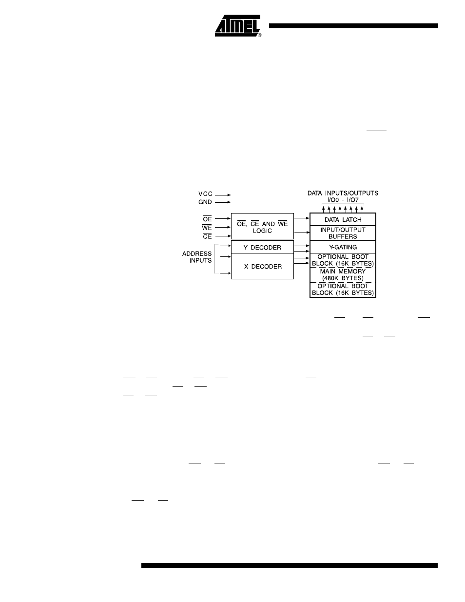
Block Diagram
Device
Operation
READ:
The AT29C040A is accessed like an EPROM. When CE and OE are low and WE is
high, the data stored at the memory location determined by the address pins is asserted on
the outputs. The outputs are put in the high impedance state whenever CE or OE is high. This
dual-line control gives designers flexibility in preventing bus contention.
BYTE LOAD:
Byte loads are used to enter the 256 bytes of a sector to be programmed or
the software codes for data protection. A byte load is performed by applying a low pulse on the
WE or CE input with CE or WE low (respectively) and OE high. The address is latched on the
falling edge of CE or WE, whichever occurs last. The data is latched by the first rising edge of
CE or WE.
PROGRAM:
The device is reprogrammed on a sector basis. If a byte of data within a sector
is to be changed, data for the entire sector must be loaded into the device. Any byte that is not
loaded during the programming of its sector will be erased to read FFH. Once the bytes of a
sector are loaded into the device, they are simultaneously programmed during the internal
programming period. After the first data byte has been loaded into the device, successive
bytes are entered in the same manner. Each new byte to be programmed must have its high
to low transition on WE (or CE) within 150
µs of the low to high transition of WE (or CE) of the
preceding byte. If a high to low transition is not detected within 150
µs of the last low to high
transition, the load period will end and the internal programming period will start. A8 to A18
specify the sector address. The sector address must be valid during each high to low transition
of WE (or CE). A0 to A7 specify the byte address within the sector. The bytes may be loaded
in any order; sequential loading is not required. Once a programming operation has been initi-
ated, and for the duration of t
WC
, a read operation will effectively be a polling operation.