Absolute maximum ratings, Dc and ac operating range, Dc characteristics – Rainbow Electronics AT45DB642 User Manual
Page 14
14
AT45DB642
1638F–DFLSH–09/02
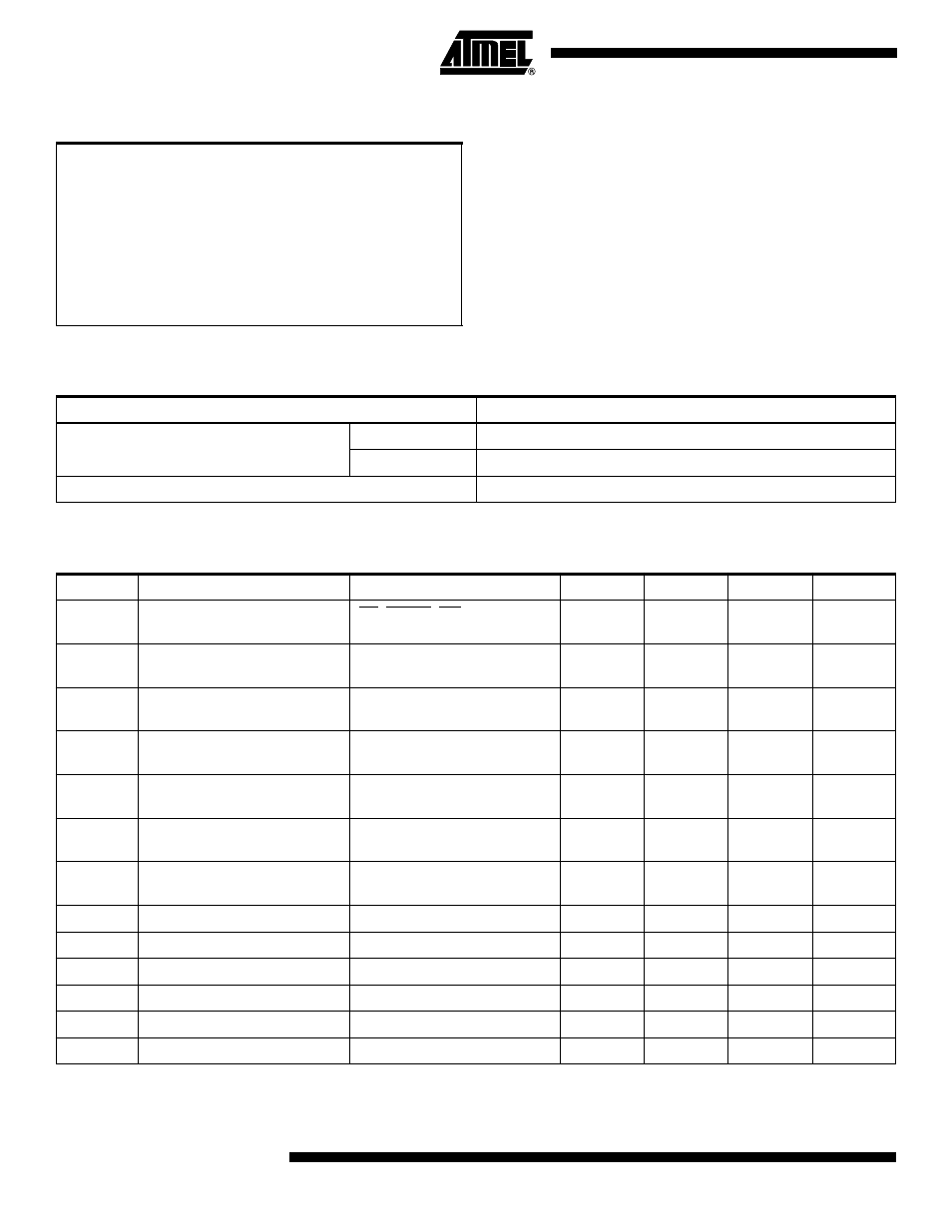
Note:
1. After power is applied and V
CC
is at the minimum specified datasheet value, the system should wait 20 ms before an opera-
tional mode is started.
Notes:
1. I
CC1
during a buffer read is 20 mA maximum.
2. I
CC2
during a buffer read is 25 mA maximum.
Absolute Maximum Ratings*
Temperature under Bias ................................ -55
°C to +125°C
*NOTICE:
Stresses beyond those listed under “Absolute
Maximum Ratings” may cause permanent dam-
age to the device. This is a stress rating only and
functional operation of the device at these or any
other conditions beyond those indicated in the
operational sections of this specification is not
implied. Exposure to absolute maximum rating
conditions for extended periods may affect
device reliability.
Storage Temperature ..................................... -65
°C to +150°C
All Input Voltages
(including NC Pins)
with Respect to Ground ...................................-0.6V to +6.25V
All Output Voltages
with Respect to Ground .............................-0.6V to V
CC
+ 0.6V
DC and AC Operating Range
AT45DB642
Operating Temperature (Case)
Com.
0
°C to 70°C
Ind.
-40
°C to 85°C
V
CC
Power Supply
(1)
2.7V to 3.6V
DC Characteristics
Symbol
Parameter
Condition
Min
Typ
Max
Units
I
SB
Standby Current
CS, RESET, WP = V
IH
, all
inputs at CMOS levels
2
10
µA
I
CC1
(1)
Active Current, Read
Operation, Serial Interface
f = 20 MHz; I
OUT
= 0 mA;
V
CC
= 3.6V
4
10
mA
I
CC2
(2)
Active Current, Read
Operation, Parallel Interface
f = 5 MHz; I
OUT
= 0 mA;
V
CC
= 3.6V
8
15
mA
I
CC3
Active Current, Program
Operation, Page Program
V
CC
= 3.6V
20
35
mA
I
CC4
Active Current, Program
Operation, Fast Page Program
V
CC
= 3.6V
30
50
mA
I
CC5
Active Current, Erase
Operation, Page
V
CC
= 3.6V
20
35
mA
I
CC6
Active Current, Erase
Operation, Block
V
CC
= 3.6V
20
35
mA
I
LI
Input Load Current
V
IN
= CMOS levels
1
µA
I
LO
Output Leakage Current
V
I/O
= CMOS levels
1
µA
V
IL
Input Low Voltage
0.6
V
V
IH
Input High Voltage
2.0
V
V
OL
Output Low Voltage
I
OL
= 1.6 mA; V
CC
= 2.7V
0.4
V
V
OH
Output High Voltage
I
OH
= -100 µA
V
CC
- 0.2V
V