A.c. characteristics, Functional description, Ht24lc04 – Rainbow Electronics HT24LC04 User Manual
Page 3
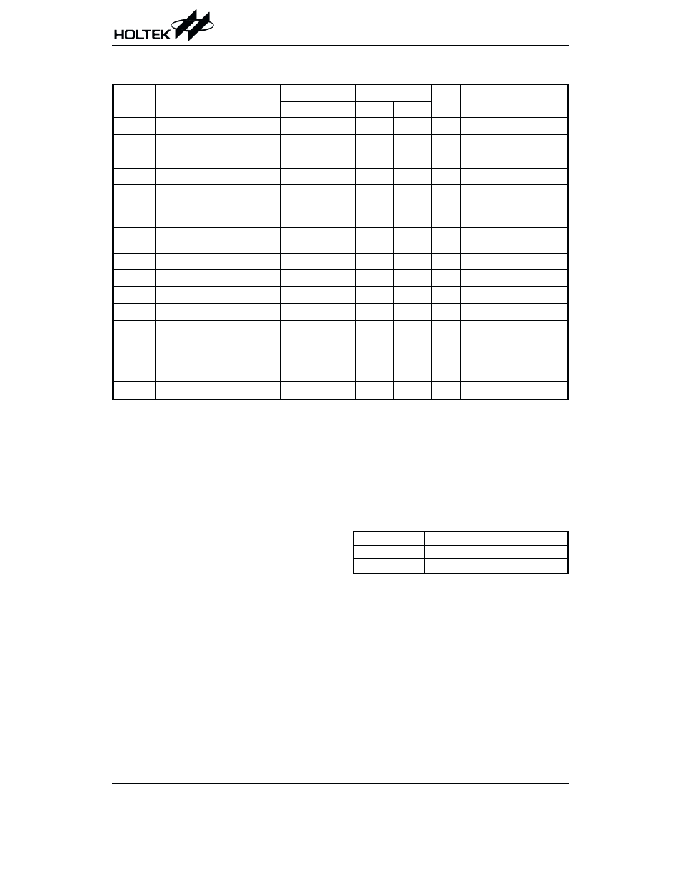
A.C. Characteristics
Ta=0
°C to 70°C
Symbol
Parameter
Standard Mode*
V
CC
=5V
±10%
Unit
Remark
Min.
Max.
Min.
Max.
f
SK
Clock Frequency
¾
100
¾
400
kHz
¾
t
HIGH
Clock High Time
4000
¾
600
¾
ns
¾
t
LOW
Clock Low Time
4700
¾
1200
¾
ns
¾
t
R
SDA and SCL Rise Time
¾
1000
¾
300
ns
Note
t
F
SDA and SCL Fall Time
¾
300
¾
300
ns
Note
t
HD:STA
START Condition Hold Time
4000
¾
600
¾
ns
After this period the first
clock pulse is generated
t
SU:STA
START Condition Setup Time
4000
¾
600
¾
ns
Only relevant for repeated
START condition
t
HD:DAT
Data Input Hold Time
0
¾
0
¾
ns
¾
t
SU:DAT
Data Input Setup Time
200
¾
100
¾
ns
¾
t
SU:STO
STOP Condition Setup Time
4000
¾
600
¾
ns
¾
t
AA
Output Valid from Clock
¾
3500
¾
900
ns
¾
t
BUF
Bus Free Time
4700
¾
1200
¾
ns
Time in which the bus
must be free before a new
transmission can start
t
SP
Input Filter Time Constant
(SDA and SCL Pins)
¾
100
¾
50
ns
Noise suppression time
t
WR
Write Cycle Time
¾
5
¾
5
ms
¾
Note:
These parameters are periodically sampled but not 100% tested
* The standard mode means V
CC
=2.2V to 5.5V
For relative timing, refer to timing diagrams
HT24LC04
Rev. 1.20
3
November 5, 2002
Functional Description
·
Serial clock (SCL)
The SCL input is used for positive edge clock data into
each EEPROM device and negative edge clock data
out of each device.
·
Serial data (SDA)
The SDA pin is bidirectional for serial data transfer.
The pin is open-drain driven and may be wired-OR
with any number of other open-drain or open collector
devices.
·
A0, A1, A2
The HT24LC04 uses the A2 and A1 inputs for hard
wire addressing and a total of four 4K devices may be
addressed on a single bus system. The A0 pin is not
connected. (The device addressing is discussed in
detail under the Device Addressing section).
·
Write protect (WP)
The HT24LC04 has a write protect pin that provides
hardware data protection. The write protect pin allows
normal read/write operations when connected to the
V
SS
. When the write protect pin is connected to Vcc,
the write protection feature is enabled and operates
as shown in the following table.
WP Pin Status
Protect Array
At V
CC
Full Array (4K)
At V
SS
Normal Read/Write Operations
Memory organization
·
HT24LC04, 4K Serial EEPROM
Internally organized with 512 8-bit words, random
word addressing requires a 9-bit data word address.
Device operations
·
Clock and data transition
Data transfer may be initiated only when the bus is not
busy. During data transfer, the data line must remain
stable whenever the clock line is high. Changes in
data line while the clock line is high will be interpreted
as a START or STOP condition.