Block diagram – Rainbow Electronics AT49LV001NT User Manual
Page 2

AT49BV/LV001(N)(T)
2
AT49BV/LV001N(T) pin 1 for the DIP and PLCC packages
and pin 9 for the TSOP package are don’t connect pins.
To allow for simple in-system reprogrammability, the
AT49BV/LV001(N)(T) does not require high input voltages
for programming. Three-volt-only commands determine the
read and programming operation of the device. Reading
data out of the device is similar to reading from an EPROM;
it has standard CE, OE, and WE inputs to avoid bus con-
tention. Reprogramming the AT49BV/LV001(N)(T) is per-
formed by erasing a block of data and then programming
on a byte-by-byte basis. The byte programming time is a
fast 50 µs. The end of a program cycle can be optionally
detected by the DATA polling feature. Once the end of a
byte program cycle has been detected, a new access for a
read or program can begin. The typical number of program
and erase cycles is in excess of 10,000 cycles.
The device is erased by executing the erase command
sequence; the device internally controls the erase opera-
tions. There are two 8K byte parameter block sections and
two main memory blocks.
The device has the capability to protect the data in the boot
block; this feature is enabled by a command sequence.
The 16K byte boot block section includes a reprogramming
lock out feature to provide data integrity. The boot sector is
designed to contain user secure code, and when the fea-
ture is enabled, the boot sector is protected from being
reprogrammed.
In the AT49BV/LV001N(T), once the boot block program-
ming lockout feature is enabled, the contents of the boot
block are permanent and cannot be changed. In the
AT49BV/LV001(T), once the boot block programming lock-
out feature is enabled, the contents of the boot block can-
not be changed with input voltage levels of 5.5 volts or less.
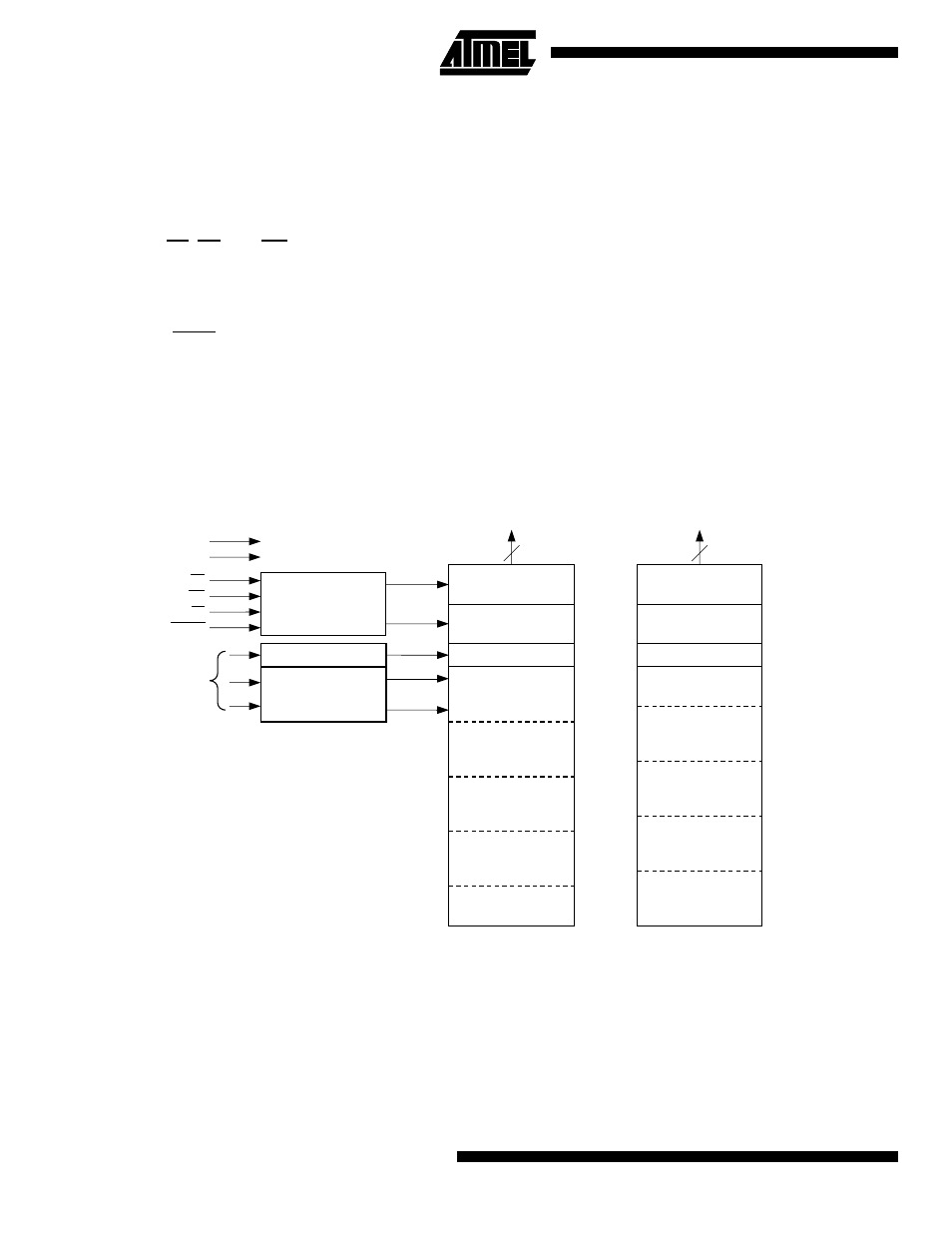
Block Diagram
CONTROL
LOGIC
Y DECODER
PARAMETER
BLOCK 1
(8K BYTES)
BOOT BLOCK
(16K BYTES)
OE
WE
CE
RESET
ADDRESS
INPUTS
VCC
GND
AT49BV/LV001(N)
DATA INPUTS/OUTPUTS
I/O7 - I/O0
8
X DECODER
PARAMETER
BLOCK 2
(8K BYTES)
MAIN MEMORY
BLOCK 1
(32K BYTES)
MAIN MEMORY
BLOCK 2
(64K BYTES)
PROGRAM
DATA LATCHES
Y-GATING
INPUT/OUTPUT
BUFFERS
1FFFF
10000
0FFFF
08000
07FFF
06000
05FFF
04000
03FFF
00000
PARAMETER
BLOCK 1
(8K BYTES)
BOOT BLOCK
(16K BYTES)
AT49BV/LV001(N)T
DATA INPUTS/OUTPUTS
I/O7 - I/O0
8
PARAMETER
BLOCK 2
(8K BYTES)
MAIN MEMORY
BLOCK 1
(32K BYTES)
MAIN MEMORY
BLOCK 2
(64K BYTES)
PROGRAM
DATA LATCHES
Y-GATING
INPUT/OUTPUT
BUFFERS
1FFFF
1C000
1BFFF
1A000
19FFF
18000
17FFF
10000
0FFFF
00000
