Rainbow Electronics AT29C010A User Manual
Features, Description, Pin configurations
1
Features
•
Fast Read Access Time – 70 ns
•
5-volt Only Reprogramming
•
Sector Program Operation
– Single Cycle Reprogram (Erase and Program)
– 1024 Sectors (128 Bytes/sector)
– Internal Address and Data Latches for 128 Bytes
•
Two 8K Bytes Boot Blocks with Lockout
•
Internal Program Control and Timer
•
Hardware and Software Data Protection
•
Fast Sector Program Cycle Time – 10 ms
•
DATA Polling for End of Program Detection
•
Low Power Dissipation
– 50 mA Active Current
– 100 µA CMOS Standby Current
•
Typical Endurance > 10,000 Cycles
•
Single 5V ±
10% Supply
•
CMOS and TTL Compatible Inputs and Outputs
•
Commercial and Industrial Temperature Ranges
Description
The AT29C010A is a 5-volt-only in-system Flash programmable and erasable read
only memory (PEROM). Its 1 megabit of memory is organized as 131,072 words by
8 bits. Manufactured with Atmel’s advanced nonvolatile CMOS technology, the device
offers access times to 70 ns with power dissipation of just 275 mW over the commer-
cial temperature range. When the device is deselected, the CMOS standby current is
1-Megabit
(128K x 8)
5-volt Only
Flash Memory
AT29C010A
Rev. 0394D–FLASH–05/02
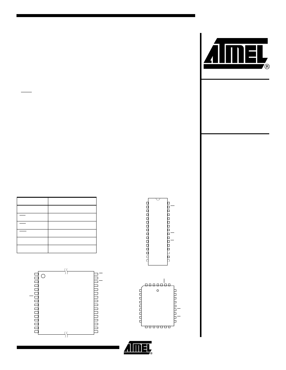
Pin Configurations
Pin Name
Function
A0 - A16
Addresses
CE
Chip Enable
OE
Output Enable
WE
Write Enable
I/O0 - I/O7
Data Inputs/Outputs
NC
No Connect
TSOP Top View
Type 1
1
2
3
4
5
6
7
8
9
10
11
12
13
14
15
16
32
31
30
29
28
27
26
25
24
23
22
21
20
19
18
17
A11
A9
A8
A13
A14
NC
WE
VCC
NC
A16
A15
A12
A7
A6
A5
A4
OE
A10
CE
I/O7
I/O6
I/O5
I/O4
I/O3
GND
I/O2
I/O1
I/O0
A0
A1
A2
A3
PLCC Top View
5
6
7
8
9
10
11
12
13
29
28
27
26
25
24
23
22
21
A7
A6
A5
A4
A3
A2
A1
A0
I/O0
A14
A13
A8
A9
A11
OE
A10
CE
I/O7
4
3
2
1
32
31
30
14
15
16
17
18
19
20
I/O1
I/O2
GND
I/O3
I/O4
I/O5
I/O6
A12
A15
A16
NC
VCC
WE
NC
DIP Top View
1
2
3
4
5
6
7
8
9
10
11
12
13
14
15
16
32
31
30
29
28
27
26
25
24
23
22
21
20
19
18
17
NC
A16
A15
A12
A7
A6
A5
A4
A3
A2
A1
A0
I/O0
I/O1
I/O2
GND
VCC
WE
NC
A14
A13
A8
A9
A11
OE
A10
CE
I/O7
I/O6
I/O5
I/O4
I/O3
Document Outline
- Pin Configurations
- Features
- Description
- Block Diagram
- Device Operation
- Absolute Maximum Ratings*
- DC and AC Operating Range
- Operating Modes
- DC Characteristics
- AC Read Characteristics
- AC Read Waveforms(1)(2)(3)(4)
- Input Test Waveforms and Measurement Level
- Output Test Load
- Pin Capacitance
- AC Byte Load Characteristics
- AC Byte Load Waveforms
- Program Cycle Characteristics
- Program Cycle Waveforms(1)(2)(3)
- Software Data Protection Enable Algorithm(1)
- Software Data Protection Disable Algorithm(1)
- Software Protected Program Cycle Waveform(1)(2)(3)
- Data Polling Characteristics(1)
- Data Polling Waveforms
- Toggle Bit Characteristics(1)
- Toggle Bit Waveforms(1)(2)(3)
- Software Product Identification Entry(1)
- Software Product Identification Exit(1)
- Boot Block Lockout Feature Enable Algorithm(1)
- Ordering Information
- Packaging Information