Rainbow Electronics DS1258Y_AB User Manual
Page 2
DS1258Y/AB
100395 2/9
READ MODE
The DS1258 devices execute a read cycle whenever
WE (Write Enable) is inactive (high) and either/both of
CEU or CEL (Chip Enables) are active (low) and OE
(Output Enable) is active (low). The unique address
specified by the 17 address inputs (A0–A16) defines
which of the 131,072 words of data is accessed. The
status of CEU and CEL determines whether all or part of
the addressed word is accessed. If CEU is active with
CEL inactive, then only the upper byte of the addressed
word is accessed. If CEU is inactive with CEL active,
then only the lower byte of the addressed word is
accessed. If both the CEU and CEL inputs are active
(low), then the entire 16 bit word is accessed. Valid data
will be available to the 16 data output drivers within t
ACC
(Access Time) after the last address input signal is
stable, providing that CEU, CEL and OE access times
are also satisfied. If OE, CEU, and CEL access times
are not satisfied, then data access must be measured
from the later occuring signal, and the limiting parame-
ter is either t
CO
for CEU, CEL, or t
OE
for OE rather than
address access.
WRITE MODE
The DS1258 devices execute a write cycle whenever
WE and either/both of CEU or CEL are active (low) after
address inputs are stable. The unique address speci-
fied by the 17 address inputs (A0–A16) defines which of
the 131,072 words of data is accessed. The status of
CEU and CEL determines whether all or part of the
addressed word is accessed. If CEU is active with CEL
inactive, then only the upper byte of the addressed word
is accessed. If CEU is inactive with CEL active, then
only the lower byte of the addressed word is accessed.
If both the CEU and CEL inputs are active (low), then the
entire 16–bit word is accessed. The write cycle is termi-
nated by the earlier rising edge of CEU and/or CEL, or
WE. All address inputs must be kept valid throughout
the write cycle. WE must return to the high state for a
minimum recovery time (t
WR
) before another cycle can
be initiated. The OE control signal should be kept inac-
tive (high) during write cycles to avoid bus contention.
However, if the output drivers are enabled (CEU and/or
CEL, and OE active) then WE will disable the outputs in
t
ODW
from its falling edge.
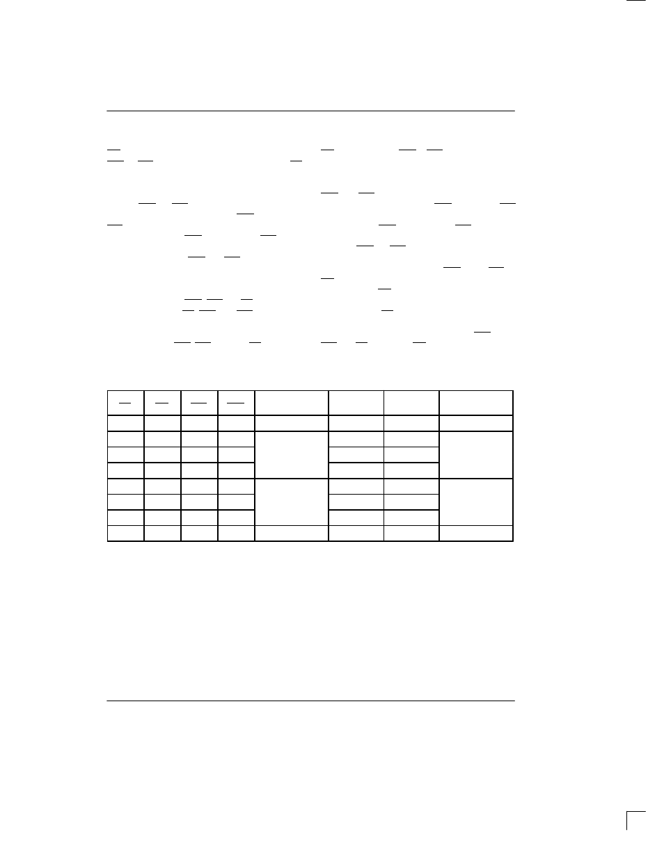
READ/WRITE FUNCTION Table 1
OE
WE
CEL
CEU
V
CC
CURRENT
DQ0–DQ7
DQ8–DQ15
CYCLE
PERFORMED
H
H
X
X
I
CCO
High–Z
High–Z
Output Disabled
L
H
L
L
I
Output
Output
R
d C
l
L
H
L
H
I
CCO
Output
High–Z
Read Cycle
L
H
H
L
High–Z
Output
X
L
L
L
I
Input
Input
W i
C
l
X
L
L
H
I
CCO
Input
High–Z
Write Cycle
X
L
H
L
High–Z
Input
X
X
H
H
I
CCS
High–Z
High–Z
Output Disabled