Pin description – Rainbow Electronics DS2482-800 User Manual
Page 4
DS2482-800: Eight-Channel 1-Wire Master
4 of 22
PIN DESCRIPTION
Note 1:
Operating current with 1-Wire write byte sequence followed by continuous Read of Status Register at
400KHz in Overdrive.
Note 2:
With standard speed the total capacitive load of the 1-Wire bus should not exceed 1nF, otherwise the
passive pullup on threshold V
IL1
may not be reached in the available time. With Overdrive speed the
capacitive load on the 1-Wire bus must not exceed 300pF.
Note 3:
Active pullup guaranteed to turn on between V
IL1MAX
and V
IH1MIN
.
Note 4:
Active or resistive pullup choice is configurable.
Note 5:
Fall time high to low (t
F1
) is derived from PD
SRC,
referenced from 0.9 × V
CC
to 0.1 × V
CC
.
Note 6:
These values apply at full load, i. e., 1nF at standard speed and 0.3nF at Overdrive speed. For
reduced load, the pulldown slew rate is slightly faster.
Note 7:
Presence pulse masking only applies to standard speed.
Note 8:
All I²C timing values are referred to V
IHmin
and V
ILmax
levels.
Note 9:
Applies to SDA, SCL, and AD0, AD1, AD2.
Note 10:
I/O pins of the DS2482 do not obstruct the SDA and SCL lines if V
CC
is switched off.
Note 11:
The DS2482 provides a hold time of at least 300ns for the SDA signal (referred to the V
IHmin
of the SCL
signal) to bridge the undefined region of the falling edge of SCL.
Note 12:
The maximum t
HD
:
DAT
has only to be met if the device does not stretch the LOW period (t
LOW
) of the
SCL signal.
Note 13:
A Fast-mode I²C-bus device can be used in a standard-mode I²C-bus system, but the requirement
t
SU
:
DAT
³250ns must then be met. This is automatically the case if the device does not stretch the LOW
period of the SCL signal. If such a device does stretch the LOW period of the SCL signal, it must
output the next data bit to the SDA line tr max + t
SU
:
DAT
= 1000 + 250 = 1250ns (according to the
standard-mode I²C-bus specification) before the SCL line is released.
Note 14:
C
B
= total capacitance of one bus line in pF. If mixed with HS-mode devices, faster fall-times according
to I²C-Bus Specification v2.1 are allowed.
Note 15:
I²C communication should not take place for the max t
OSCWUP
time following a power-on reset.
Note 16:
Except for t
F1
, all 1-Wire timing specifications and t
APUOT
are derived from the same timing circuit.
Therefore, if one of these parameters is found to be off the typical value, it is safe to assume that all of
these parameters deviate from their typical value in the same direction and by the same degree.
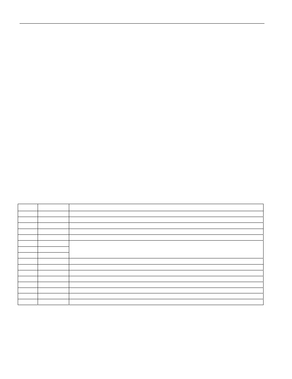
PIN NAME
FUNCTION
1
IO3
IO Driver for 1-Wire Line #3
2
SCL
I²C Serial Clock Input; must be tied to VCC through a pullup resistor.
3
SDA
I²C Serial Data Input/Output; must be tied to VCC through a pullup resistor.
4
VCC
Power Supply Input
5 NC
Not
Connected
6 AD2
7 AD1
8 AD0
I²C Address Inputs; must be tied to VCC or GND. These inputs determine the I²C slave
address of the device, see Figure 9.
9
IO7
IO Driver for 1-Wire Line #7
10
IO6
IO Driver for 1-Wire Line #6
11
IO5
IO Driver for 1-Wire Line #5
12
IO4
IO Driver for 1-Wire Line #4
13
GND
Ground Reference
14
IO0
IO Driver for 1-Wire Line #0
15
IO1
IO Driver for 1-Wire Line #1
16
IO2
IO Driver for 1-Wire Line #2