I²c interface, Figure 8. i²c protocol overview – Rainbow Electronics DS2482-800 User Manual
Page 15
DS2482-800: Eight-Channel 1-Wire Master
15 of 22
Bit Allocation in the Direction Byte
bit 7
bit 6
bit 5
bit 4
bit 3
bit 2
bit 1
bit 0
V x x x x x x x
x = don’t care
I²C INTERFACE
General Characteristics
The I²C bus uses a data line (SDA) plus a clock signal (SCL) for communication. Both SDA and SCL are
bidirectional lines, connected to a positive supply voltage through a pullup resistor. When there is no
communication, both lines are HIGH. The output stages of devices connected to the bus must have an open-drain
or open-collector to perform the wired-AND function. Data on the I²C bus can be transferred at rates of up to
100kbps in the Standard-mode, up to 400kbps in the Fast-mode. The DS2482 works in both modes.
A device that sends data on the bus is defined as a transmitter, and a device receiving data as a receiver. The
device that controls the communication is called a “master.” The devices that are controlled by the master are
“slaves.” To be individually accessed, each device must have a slave address that does not conflict with other
devices on the bus.
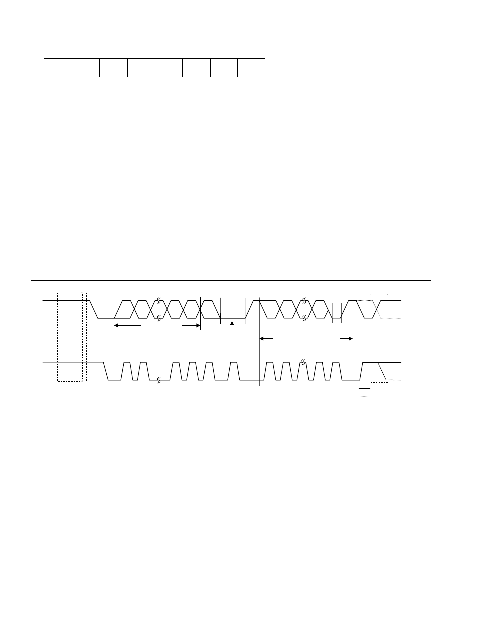
Data transfers may be initiated only when the bus is not busy. The master generates the serial clock (SCL),
controls the bus access, generates the START and STOP conditions, and determines the number of data bytes
transferred between START and STOP (Figure 8). Data is transferred in bytes with the most significant bit being
transmitted first. After each byte follows an acknowledge bit to allow synchronization between master and slave.
Figure 8. I²C Protocol Overview
SCL
SDA
1
2
6
7
8
ACK
9
9
1
2
8
MS-bit
R/W
Slave Address
ACK
bit
Acknowledgment
from Receiver
ACK
bit
START
Condition
ACK
Repeated if more bytes
are transferred
STOP Condition
Repeated START
Condition
Idle
Slave Address
The slave address to which the DS2482 responds is shown in Figure 9. The logic states at the address pins AD0,
AD1 and AD2 determine the value of the address bits A0, A1, and A2. The address pins allow the device to
respond to one of eight possible slave addresses.
The slave address is part of the slave-address/control byte. The
last bit of the slave-address/control byte (R/
W) defines the data direction. When set to a 0, subsequent data will
flow from master to slave (write access); when set to a 1, data will flow from slave to master (read access).