Rainbow Electronics DS2482-800 User Manual
Page 3
DS2482-800: Eight-Channel 1-Wire Master
3 of 22
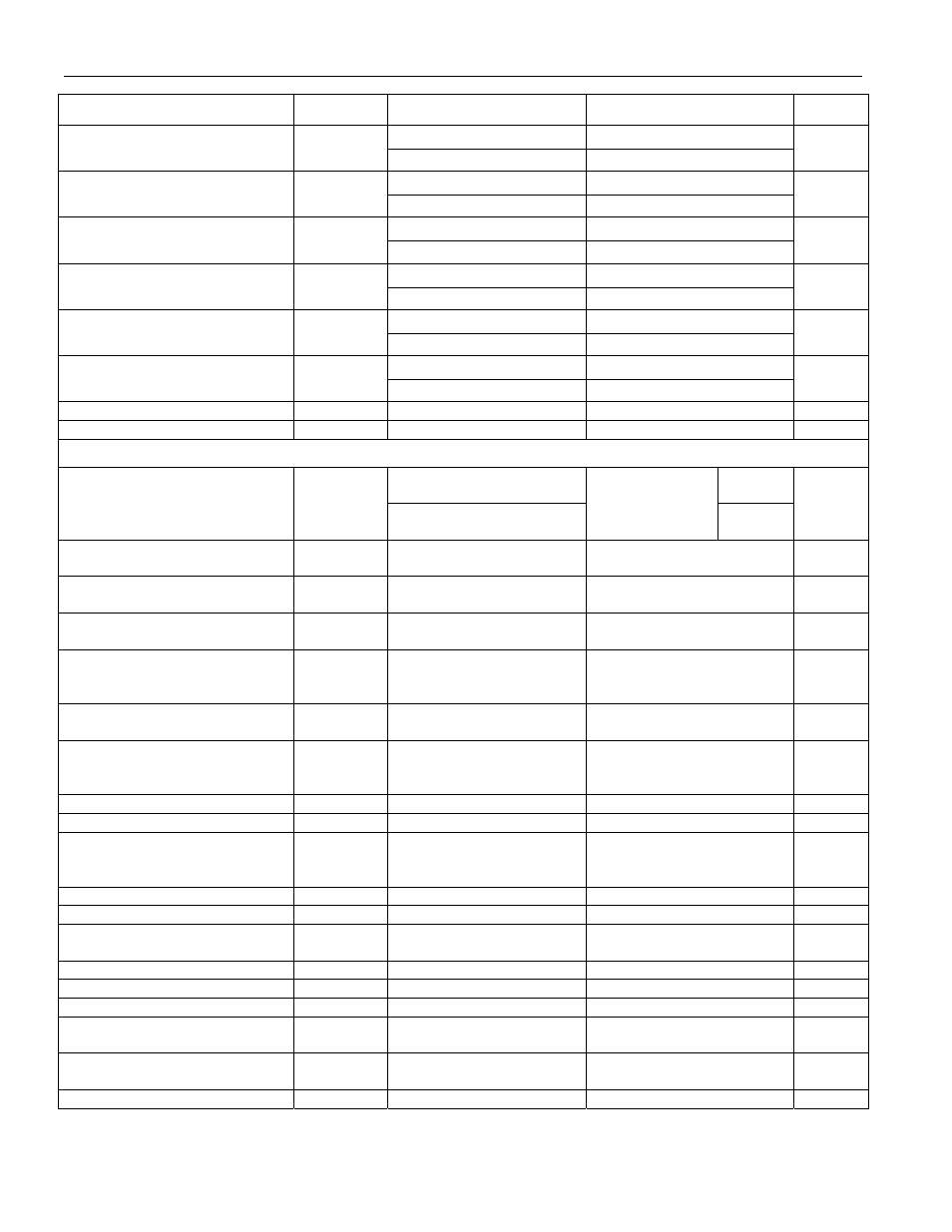
PARAMETER SYMBOL
CONDITIONS
MIN
TYP
MAX
UNITS
Standard 60
64
68
Write 0 Low Time
t
W0L
Overdrive 7.1
7.5
7.9
µs
Standard 5.0
5.3
5.6
Write 0 Recovery Time
t
REC0
Overdrive 2.8
3.0
3.2
µs
Standard 570
600
630
Reset Low Time
t
RSTL
Overdrive 68.4
72
75.6
µs
Standard 66.5
70
73.5
Presence-Detect Sample Time
t
MSP
Overdrive 7.1
7.5
7.9
µs
Standard 7.6
8
8.4
Sampling for Short and
Interrupt
t
SI
Overdrive 0.7
0.75
0.8
µs
Standard 554.8
584
613.2
Reset High Time
t
RSTH
Overdrive 70.3
74
77.7
µs
Presence Pulse Mask Start
t
ppm1
(Note
7)
9.5 10 10.5 µs
Presence Pulse Mask Stop
t
ppm2
(Note
7)
57 60 63
µs
I²C-Pins (Note 8) See Figure 10
V
CC
= 2.9V to 3.7V
0.25 ×
V
CC
LOW Level Input Voltage
V
IL
V
CC
= 4.5V to 5.5V
-0.5
0.22 ×
V
CC
V
HIGH Level Input Voltage
V
IH
0.7 ×
V
CC
V
CC
+
0.5V
V
Hysteresis of Schmitt Trigger
Inputs
V
hys
0.05 ×
V
CC
V
LOW Level Output Voltage at
3mA Sink Current
V
OL
0.4 V
Output Fall Time from V
Ihmin
to
V
ILmax
with a Bus Capacitance
from 10pF to 400pF
t
of
60 250 ns
Pulse Width of Spikes that are
Suppressed by the Input Filter
t
SP
SDA and SCL pins only
50
ns
Input Current Each I/O Pin with
an Input Voltage Between
0.1V
CCmax
and 0.9V
CCmax
I
i
(Notes
9,
10)
-10 10 µA
Input Capacitance
C
i
(Note
9)
10 pF
SCL Clock Frequency
f
SCL
0
400 kHz
Hold Time (Repeated) START
Condition. After this Period, the
First Clock Pulse is Generated.
t
HD:STA
0.6
µs
LOW Period of the SCL Clock
t
LOW
1.3
µs
HIGH Period of the SCL Clock
t
HIGH
0.6
µs
Setup Time for a Repeated
START Condition
t
SU:STA
0.6
µs
Data Hold Time
t
HD:DAT
(Notes 11, 12)
0.9
µs
Data Setup Time
t
SU:DAT
(Note
13)
250
ns
Setup Time for STOP Condition
t
SU:STO
0.6
µs
Bus Free Time Between a
STOP and START Condition
t
BUF
1.3
µs
Capacitive Load for Each Bus
Line
C
b
(Note
14)
400 pF
Oscillator Warm-Up Time
t
OSCWUP
(Note
15)
100
µs