Rainbow Electronics MAX16064 User Manual
Page 14
MAX16064
±0.3% Accurate, Quad, Power-Supply Controller with
Active-Voltage Output Control and PMBus Interface
14
______________________________________________________________________________________
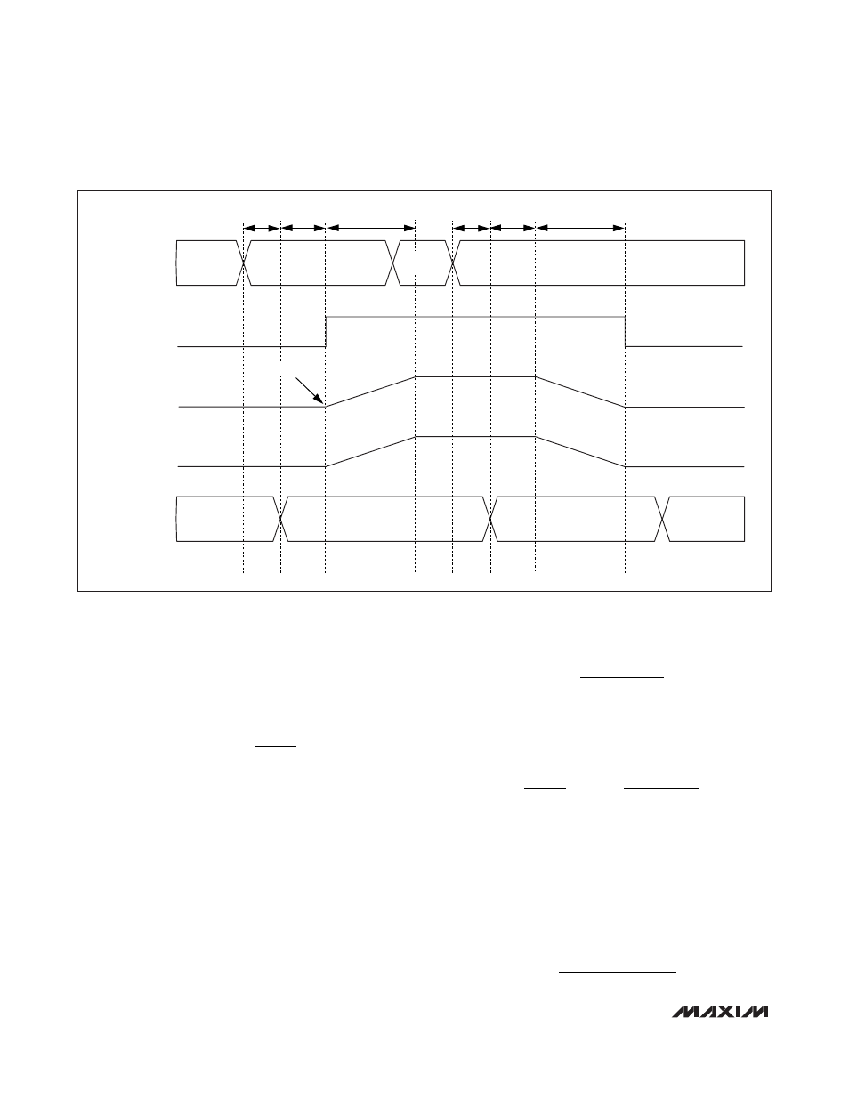
After receiving an OPERATION OFF command or a
turn-off signal from A3/CONTROL, the MAX16064 waits
the programmed t
OFF_DELAY
time, deasserts the
ENOUT_ output, and turns off the power supply.
For the FB mode, use the following formula to calculate
the value of R
FB
:
Where R
1
is the upper feedback divider resistor, ∆V
O
is
the required change in output voltage, and ∆V
DAC
is
the DACOUT output-voltage change that the user
allows. The recommended operating range for the
DACOUT_ voltage for power-supply output voltage
adjustment is between 30mV and 2V. Note that ∆V
DAC
is the difference between the steady-state power-sup-
ply FB node voltage, V
FB
, and the voltage limits on
DACOUT_. This is best illustrated with an example as
follows:
Consider an application involving a power supply with
V
FB
= 0.6V. Let the desired margining be ±10% for a
power-supply output voltage of 1V. For a power supply
with an upper voltage divider resistor R
1
= 10kΩ, R
FB
is
calculated as follows:
This value of R
FB
allows the MAX16064 to margin the
power-supply output voltage up by 10%. It is useful to
check the margin low condition by using the formula:
The effective margining range for the 57kΩ resistor
therefore turns out to be between +10% and -24.5%.
Note that the VOUT_TRANSITION_RATE parameter has
no effect on FB mode. The transition time for margining
in the FB mode of operation is a function of the update
rate (f
AVOC
), see the
MFR_DAC_ACT_CNT (E0h)
sec-
tion for the calculation of f
AVOC
. R
FB
and R
1
, and is
given by the following formula:
t
R
x
V
x
f
x R
FB
FB
O
AVOC
=
⎛
⎝
⎜
⎞
⎠
⎟
∆
2000
1
∆
∆
Ω
Ω
V
R
V
R
k
V
V
k
O
DAC
FB
=
Ч
=
Ч
=
−
1
10
2 0
0 6
57
0 24
( .
.
)
.
5
5V
R
k
V
V
V
k
FB
=
×
=
−
10
0 6
0 03
0 1
57
Ω
Ω
( .
.
)
.
R
R
V
V
FB
DAC
O
=
×
1
∆
∆
IDLE
IDLE
OPERATION
ON
t
PMB_RSP
t
ON_DELAY
t
ON_RISE
t
PMB_RSP
t
OFF_DELAY
t
ON_FALL
ENOUT_
PMBus
DAC OUTPUT
POWER-SUPPLY
V
OUT
POWER-SUPPLY
OPERATION
CLOSE S_
TURN-ON
TURN-OFF
OPERATION
OFF
Figure 4. REFIN Mode Timing