Max6901, Wire serial rtc in a tdfn, Detailed description – Rainbow Electronics MAX6901 User Manual
Page 4: Command and control, Typical operating characteristics, Pin description

MAX6901
Detailed Description
The MAX6901 is a real-time clock/calendar with a 3-wire
serial interface and 31
✕
8 bits of SRAM. It provides sec-
onds, minutes, hours, day of the week, date of the
month, month, and year information, held in seven 8-bit
timekeeping registers (Functional Diagram). An on-chip
32.768kHz oscillator circuit does not require any exter-
nal resistors or capacitors to operate. Table 1 specifies
the parameters for the external crystal, and Figure 1
shows a functional schematic of the oscillator circuit.
The MAX6901’s register addresses and definitions are
described in Tables 2 and 3. Time and calendar data
are stored in the registers in binary coded decimal
(BCD) format. A polled alarm function is included for
scheduled timing of user-defined times or intervals.
Command and Control
Address/Command Byte
Each data transfer into or out of the MAX6901 is initiat-
ed by an Address/Command byte. The Address/
Command byte specifies which registers are to be
accessed, and if the access is a read or a write. Table
2 shows the Address/Command bytes and their associ-
ated registers, and Table 3 lists the hex codes for all
read and write operations. The Address/Command
bytes are input LSB (bit 0) first. Bit 0 specifies a write
(logic 0) or read (logic 1). Bits 1 to 5 specify the desig-
nated register to be written or read. Bit 6 specifies reg-
ister data (logic 0), or RAM data (logic 1). The MSB (bit
7) must be logic 1. If the MSB is a zero, writes to the
MAX6901 are disabled.
3-Wire Serial RTC in a TDFN
4
_______________________________________________________________________________________
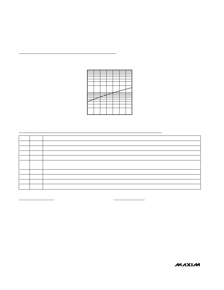
Typical Operating Characteristics
(T
A
= +25°C, unless otherwise noted.)
0.1
2.0
2.5
3.5
4.0
5.5
4.5
5.0
3.0
TIMEKEEPING CURRENT
vs. SUPPLY VOLTAGE
1.0
10.0
MAX6901 toc01
SUPPLY VOLTAGE (V)
SUPPLY CURRENT (
µ
A)
PIN
NAME
FUNCTION
1
SCLK
Serial Clock Input. 3-wire serial clock for I/O data transfers.
2
V
CC
Power-Supply Pin. Bypass V
CC
to GND with a 0.1µF capacitor.
3
X2
External 32.768kHz Crystal Connection
4
X1
External 32.768kHz Crystal Connection
5
32KHZ
Buffered Push-Pull 32.768kHz Output. When enabled, 32KHZ puts a buffered version of the timekeeping clock.
When disabled, 32KHZ is high impedance. The power-on reset (POR) default state of 32KHZ is enabled.
6
GND
Ground Connection
7
CS
Chip-Select Input. Active-high for valid data transfers.
8
I/O
Data Input/Output. 3-wire serial data input/output connection.
—
PAD
Ground
Pin Description
