Bit microcontroller with infrared module maxq613, Spi electrical characteristics (continued) – Rainbow Electronics MAXQ613 User Manual
Page 7
16-Bit Microcontroller with Infrared Module
MAXQ613
_______________________________________________________________________________________ 7
SPI ELECTRICAL CHARACTERISTICS (continued)
(V
DD
= V
RST
to 3.6V, T
A
= 0NC to +70NC, unless otherwise noted.) (Note 11)
Note 1: Specifications to 0NC are guaranteed by design and are not production tested. Typical = +25NC, V
DD
= +3.3V, unless
otherwise noted.
Note 2: V
PFW
can be programmed to the following nominal voltage trip points: 1.8V, 1.9V, 2.55V, and 2.75V ±3%. The values
listed in the Recommended Operating Conditions table are for the default configuration of 1.8V nominal.
Note 3: The power-fail reset and POR detectors are designed to operate in tandem to ensure that one or both of these signals
is active at all times when V
DD
< V
RST
, ensuring the device maintains the reset state until minimum operating voltage is
achieved.
Note 4: Guaranteed by design and not production tested.
Note 5: Measured on the V
DD
pin and the device not in reset. All inputs are connected to GND or V
DD
. Outputs do not source/
sink any current. The device is executing code from flash memory.
Note 6: The power-check interval (PCI) can be set to always on, or to 1024, 2048, or 4096 nanopower ring clock cycles.
Note 7: Current consumption during POR when powering up while V
DD
is less than the POR release voltage.
Note 8: The minimum amount of time that V
DD
must be below V
PFW
before a power-fail event is detected; refer to the MAXQ610
User’s Guide for details.
Note 9: The maximum total current, I
OH(MAX)
and I
OL(MAX)
, for all listed outputs combined should not exceed 32mA to satisfy the
maximum specified voltage drop. This does not include the IRTX output.
Note 10: Programming time does not include overhead associated with utility ROM interface.
Note 11: AC electrical specifications are guaranteed by design and are not production tested.
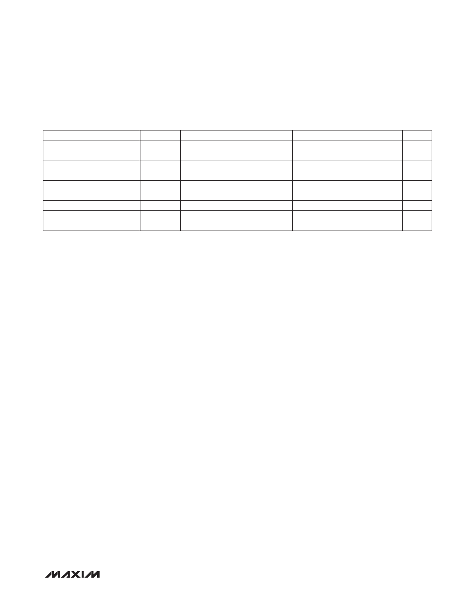
PARAMETER
SYMBOL
CONDITIONS
MIN
TYP
MAX
UNITS
MOSI Input from SCLK
Sample Edge Transition Hold
t
SIH
t
SPI_RF
ns
MISO Output Valid After SCLK
Shift Edge Transition
t
SOV
2t
SPI_RF
ns
SSEL Inactive
t
SSH
t
CK
+
t
SPI_RF
ns
SCLK Inactive to SSEL Rising
t
SD
t
SPI_RF
ns
MISO Output Disabled After
SSEL Edge Rise
t
SLH
2t
CK
+
2t
SPI_RF
ns