Bit microcontroller with infrared module maxq613, Pin description (continued) – Rainbow Electronics MAXQ613 User Manual
Page 10
16-Bit Microcontroller with Infrared Module
MAXQ613
10 _____________________________________________________________________________________
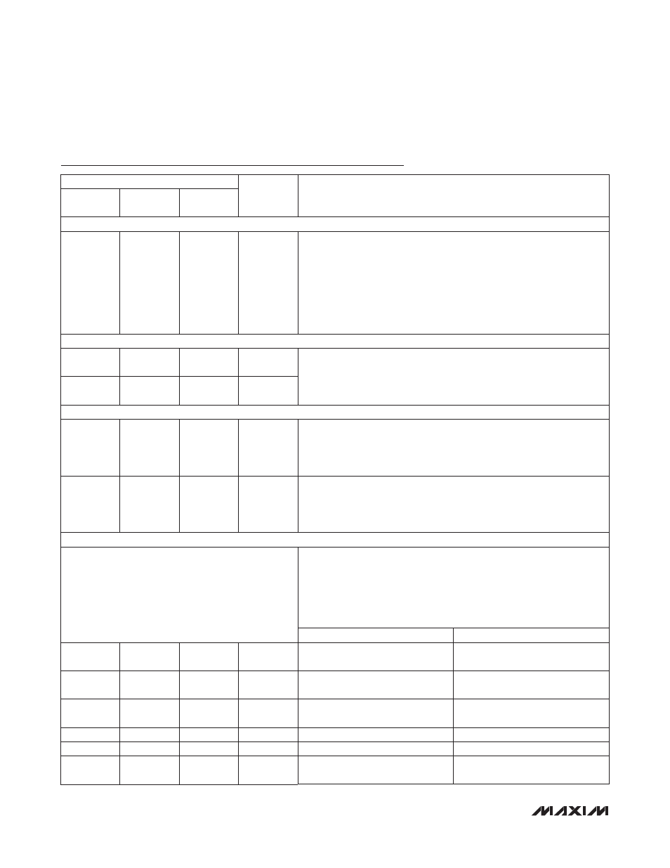
Pin Description (continued)
PIN
NAME
FUNCTION
BARE DIE
32 TQFN-
EP/LQFP
44 TQFN-
EP/TQFP
RESET PIN
35
28
40
RESET
Digital, Active-Low, Reset Input/Output. The device remains in reset
as long as this pin is low and begins executing from the utility ROM at
address 8000h when this pin returns to a high state. The pin includes
pullup current source; if this pin is driven by an external device, it should
be driven by an open-drain source capable of sinking in excess of 4mA.
This pin can be left unconnected if there is no need to place the device in
a reset state using an external signal. This pin is driven low as an output
when an internal reset condition occurs.
CLOCK PINS
20
18
23
HFXIN
High-Frequency Crystal Input. Connect an external crystal or resona-
tor between HFXIN and HFXOUT for use as the high-frequency system
clock. Alternatively, HFXIN is the input for an external, high-frequency
clock source when HFXOUT is unconnected.
21
19
24
HFXOUT
IR FUNCTION PINS
38
31
43
IRTX
IR Transmit Output. IR transmission pin capable of sinking 25mA. This
pin defaults to a high-impedance input with the weak pullup disabled
during all forms of reset. Software must configure this pin after release
from reset to remove the high-impedance input condition.
39
32
44
IRRX
IR Receive Input. This pin defaults to a high-impedance input with the
weak pullup disabled during all forms of reset. Software must configure
this pin after release from reset to remove the high-impedance input
condition.
GENERAL-PURPOSE I/O AND SPECIAL FUNCTION PINS
Port 0 General-Purpose, Digital I/O Pins. These port pins function as
general-purpose I/O pins with their input and output states controlled by
the PD0, PO0, and PI0 registers. All port pins default to high-impedance
mode after a reset. Software must configure these pins after release
from reset to remove the high-impedance condition. All alternate func-
tions must be enabled from software before they can be used.
GPIO PORT PIN
SPECIAL FUNCTION
1
1
1
P0.0/IRTXM/
INT8
P0.0
IR Modulator Output/INT8
2
2
3
P0.1/RX/
INT9
P0.1
USART Receive/INT9
3
3
5
P0.2/TX/
INT10
P0.2
USART Transmit/INT10
4
4
6
P0.3/INT11
P0.3
INT11
5
5
7
P0.4/INT12
P0.4
INT12
6
6
8
P0.5/TBA0/
TBA1/INT13
P0.5
Type B Timer 0 Pin A or Type B
Timer 1 Pin A/INT13