Absolute maximum ratings, Recommended operating conditions, Bit microcontroller with infrared module maxq613 – Rainbow Electronics MAXQ613 User Manual
Page 4
16-Bit Microcontroller with Infrared Module
MAXQ613
4 ______________________________________________________________________________________
Stresses beyond those listed under “Absolute Maximum Ratings” may cause permanent damage to the device. These are stress ratings only, and functional
operation of the device at these or any other conditions beyond those indicated in the operational sections of the specifications is not implied. Exposure to absolute
maximum rating conditions for extended periods may affect device reliability.
Voltage Range on V
DD
with Respect to GND .....-0.3V to +3.6V
Voltage Range on Any Lead with
Respect to GND Except V
DD
............... -0.3V to (V
DD
+ 0.5V)
Continuous Power Dissipation (T
A
= +70NC)
32-Pin TQFN (single-layer board)
(derate 21.3mW/NC above +70NC)..........................1702.1mW
32-Pin TQFN (multilayer board)
(derate 34.5mW/NC above +70NC)..........................2758.6mW
32-Pin LQFP (multilayer board)
(derate 20.7mW/NC above +70NC)..........................1652.9mW
44-Pin TQFN (single-layer board)
(derate 27mW/NC above +70NC).............................2162.2mW
44-Pin TQFN (multilayer board)
(derate 37mW/NC above +70NC)................................2963mW
44-Pin TQFP (multilayer board)
(derate 19mW/NC above +70NC)................................1504mW
Operating Temperature Range ............................. 0NC to +70NC
Storage Temperature Range ............................ -65NC to +150NC
Lead Temperature (excluding dice; soldering, 10s) ......+300NC
Soldering Temperature (reflow) ......................................+260NC
RECOMMENDED OPERATING CONDITIONS
(V
DD
= V
RST
to 3.6V, T
A
= 0NC to +70NC, unless otherwise noted.) (Note 1)
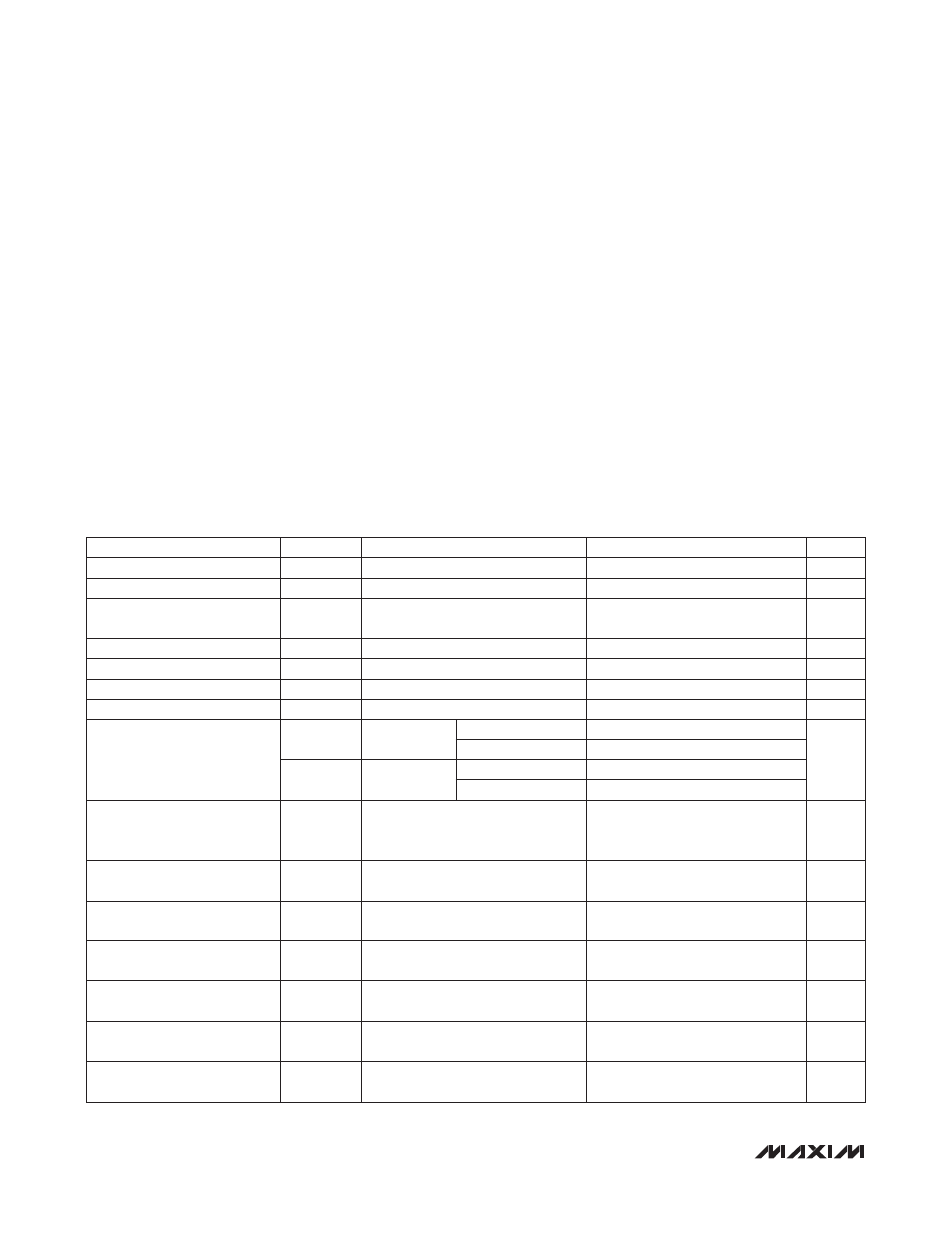
ABSOLUTE MAXIMUM RATINGS
PARAMETER
SYMBOL
CONDITIONS
MIN
TYP
MAX
UNITS
Supply Voltage
V
DD
V
RST
3.6
V
1.8V Internal Regulator
V
REG18
1.62
1.8
1.98
V
Power-Fail Warning Voltage for
Supply
V
PFW
Monitors V
DD
(Note 2)
1.75
1.8
1.85
V
Power-Fail Reset Voltage
V
RST
Monitors V
DD
(Note 3)
1.64
1.67
1.70
V
POR Voltage
V
POR
Monitors V
DD
1
1.42
V
RAM Data-Retention Voltage
V
DRV
(Note 4)
1.0
V
Active Current
I
DD_1
Sysclk = 12MHz (Note 5)
3.25
4
mA
Stop-Mode Current
I
S1
Power-Fail Off
T
A
= +25NC
0.2
2.0
F
A
T
A
= 0
°C to +70NC
0.2
8
I
S2
Power-Fail On
T
A
= +25NC
22
29.5
T
A
= 0
°C to +70NC
27.6
42
Current Consumption During
Power-Fail
I
PFR
(Note 6)
[(3 x I
S2
) +
((PCI - 3) x (I
S1
+
I
NANO
))]/PCI
F
A
Power Consumption During
POR
I
POR
(Note 7)
100
nA
Stop-Mode Resume Time
t
ON
375 + (8192 x
t
HFXIN)
F
s
Power-Fail Monitor Startup
Time
t
PFM_ON
(Note 4)
150
F
s
Power-Fail Warning Detection
Time
t
PFW
(Note 8)
10
F
s
Input Low Voltage for IRTX,
IRRX, RESET, and All Port Pins
V
IL
V
GND
0.3 x V
DD
V
Input High Voltage for IRTX,
IRRX, RESET, and All Port Pins
V
IH
0.7 x V
DD
V
DD
V