T5754, Application circuit – Rainbow Electronics T5754 User Manual
Page 5
5
T5754
4511D–RKE–08/02
Output Matching and Power
Setting
The output power is set by the load impedance of the antenna. The maximum output
power is achieved with a load impedance of Z
Load,opt
= (166 + j223)
W
. There must be a
low resistive path to V
S
to deliver the DC current.
The delivered current pulse of the power amplifier is 9 mA and the maximum output
power is delivered to a resistive load of 465
W
if the 1.0 pF output capacitance of the
power amplifier is compensated by the load impedance.
An optimum load impedance of:
Z
Load
= 465
W
|| j/(2
´ p
1.0 pF) = (166 + j223)
W
thus results for the maximum output
power of 7.5 dBm.
The load impedance is defined as the impedance seen from the T5754’s ANT1, ANT2
into the matching network. Do not confuse this large signal load impedance with a small
signal input impedance delivered as input characteristic of RF amplifiers and measured
from the application into the IC instead of from the IC into the application for a power
amplifier.
Less output power is achieved by lowering the real parallel part of 465
W
where the
parallel imaginary part should be kept constant.
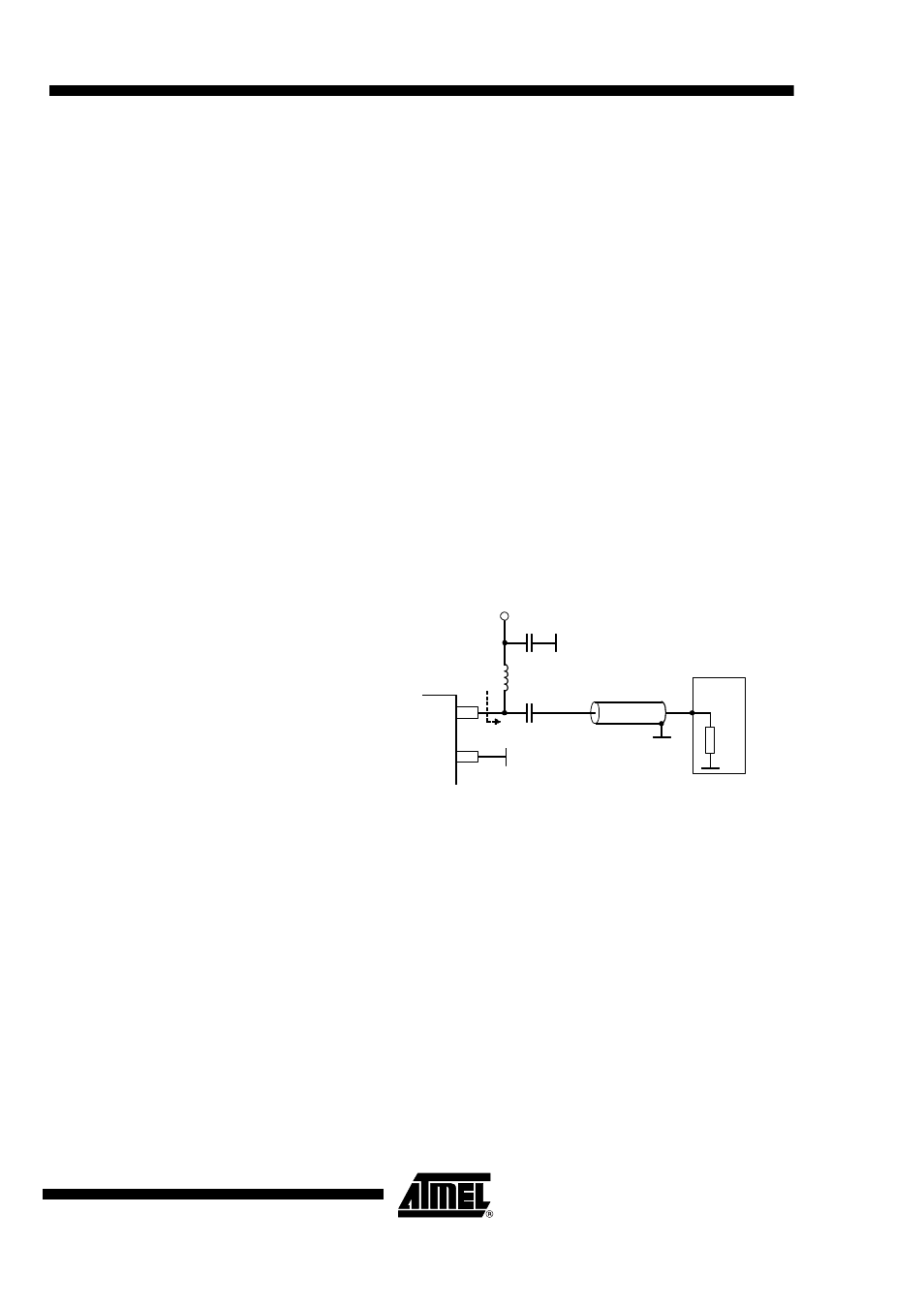
Output power measurement can be done with the circuit of Figure 5. Note that the com-
ponent values must be changed to compensate the individual board parasitics until the
T5754 has the right load impedance Z
Load,opt
= (166 + j223)
W
. Also the damping of the
cable used to measure the output power must be calibrated out.
Figure 5.
Output Power Measurement
Application Circuit
For the supply-voltage blocking capacitor C
3
a value of 68 nF/X7R is recommended
(see Figure 6 and Figure 7). C
1
and C
2
are used to match the loop antenna to the power
amplifier where C
1
typically is 8.2 pF/NP0 and C
2
is 6 pF/NP0 (10 pF + 15 pF in series);
for C
2
two capacitors in series should be used to achieve a better tolerance value and to
have the possibility to realize the Z
Load,opt
by using standard valued capacitors.
C
1
forms together with the pins of T5754 and the PCB board wires a series resonance
loop that suppresses the 1
st
harmonic, hence the position of C
1
on the PCB is important.
Normally the best supression is achieved when C
1
is placed as close as possible to the
Pins ANT1 and ANT2.
The loop antenna should not exceed a width of 1.5 mm, otherwise the Q-factor of the
loop antenna is too high.
L
1
(
[
50 nH to 100 nH) can be printed on PCB. C
4
should be selected that the XTO runs
on the load resonance frequency of the crystal. Normally, a value of 12 pF results for a
15 pF load-capacitance crystal.
~
~
ANT2
ANT1
Rin
Power
meter
C
1
= 1n
L
1
= 33n
C
2
= 2.2p
Z
Lopt
V
S
Z = 50
W
50
W