T5754, General description – Rainbow Electronics T5754 User Manual
Page 3
3
T5754
4511D–RKE–08/02
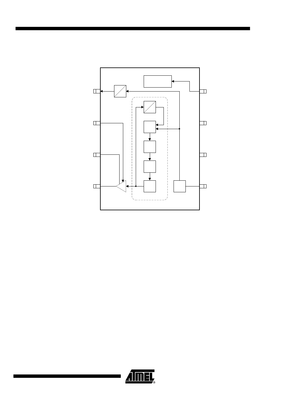
Figure 3.
Block Diagram
General Description
This fully integrated PLL transmitter allows particularly simple, low-cost RF miniature
transmitters to be assembled. The VCO is locked to 32 f
XTAL
hence a 13.56 MHz crystal
is needed for a 433.92 MHz transmitter. All other PLL and VCO peripheral elements are
integrated.
The XTO is a series resonance oscillator so that only one capacitor together with a
crystal connected in series to GND are needed as external elements.
The crystal oscillator together with the PLL needs typically <1 ms until the PLL is locked
and the CLK output is stable. There is a wait time of
³
1 ms until the CLK is used for the
microcontroller and the PA is switched on.
The power amplifier is an open-collector output delivering a current pulse which is nearly
independent from the load impedance. The delivered output power is hence controllable
via the connected load impedance.
This output configuration enables a simple matching to any kind of antenna or to 50
W
. A
high power efficiency of
h
= P
out
/(I
S,PA
V
S
) of 36% for the power amplifier results when
an optimized load impedance of Z
Load
= (166 + j223)
W
is used at 3 V supply voltage.
CLK
PA_ENABLE
ANT2
ANT1
ENABLE
GND
VS
XTAL
1
2
3
4
5
6
7
8
VCO
LF
CP
f
32
XTO
PLL
PA
f
4
Power up / down
T5754
PFD