Detailed description, Table 1. dc-balance programming – Rainbow Electronics MAX9216 User Manual
Page 6
Detailed Description
The MAX9210/MAX9212/MAX9220 operate at a parallel
clock frequency of 8MHz to 34MHz in DC-balanced
mode and 10MHz to 40MHz in non-DC-balanced
mode. The MAX9214/MAX9216/MAX9222 operate at a
parallel clock frequency of 16MHz to 66MHz in DC-bal-
anced mode and 20MHz to 85MHz in non-DC-bal-
anced mode. The transition times of the single-ended
outputs are increased on the MAX9210/MAX9212/
MAX9220 for reduced EMI.
DC-balanced or non-DC-balanced operation is con-
trolled by the DCB/NC pin (see Table 1 for DCB/NC
default settings and operating modes). In non-DC-bal-
anced mode, each channel deserializes 7 bits every
cycle of the parallel clock. In DC-balanced mode, 9 bits
are deserialized every clock cycle (7 data bits + 2 DC-
balance bits). The highest data rate in DC-balanced
mode for the MAX9214, MAX9216, and MAX9222 is
66MHz x 9 = 594Mbps. In non-DC-balanced mode, the
maximum data rate is 85MHz x 7 = 595Mbps.
DC Balance
Data coding by the MAX9209/MAX9211/MAX9213/
MAX9215 serializers (which are companion devices to
the MAX9210/MAX9212/MAX9214/MAX9216/MAX9220/
MAX9222 deserializers) limits the imbalance of ones
and zeros transmitted on each channel. If +1 is assigned
to each binary 1 transmitted and -1 is assigned to each
binary 0 transmitted, the variation in the running sum of
assigned values is called the digital sum variation
(DSV). The maximum DSV for the data channels is 10.
At most, 10 more zeros than ones, or 10 more ones than
zeros, are transmitted. The maximum DSV for the clock
MAX9210/MAX9212/MAX9214/MAX9216/MAX9220/MAX9222
Programmable DC-Balance
21-Bit Deserializers
6
_______________________________________________________________________________________
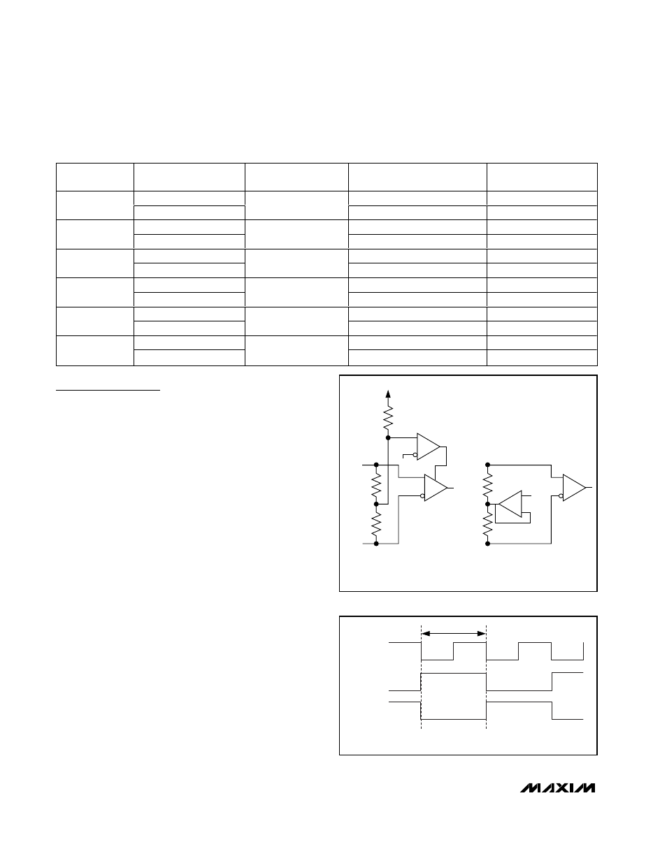
V
CC
- 0.3V
V
CC
RIN2
RIN1
RxIN_ + OR
RxCLK IN+
RxIN_ - OR
RxCLK IN-
RIN1
RIN1
RxIN_ + OR
RxCLK IN+
RxIN_ - OR
RxCLK IN-
RIN1
NON-DC-BALANCED MODE
DC-BALANCED MODE
1.2V
Figure 1. LVDS Input Circuits
Table 1. DC-Balance Programming
DEVICE
DCB/NC
OUTPUT STROBE
EDGE
OPERATING MODE
OPERATING
FREQUENCY (MHz)
High or open
DC balanced
8 to 34
MAX9210
Low
Rising
Non-DC balanced
10 to 40
High
DC balanced
8 to34
MAX9212
Low or open
Rising
Non-DC balanced
10 to 40
High or open
DC balanced
16 to 66
MAX9214
Low
Rising
Non-DC balanced
20 to 85
High
DC balanced
16 to 66
MAX9216
Low or open
Rising
Non-DC balanced
20 to 85
High or open
DC balanced
8 to 34
MAX9220
Low
Falling
Non-DC balanced
10 to 40
High or open
DC balanced
16 to 66
MAX9222
Low
Falling
Non-DC balanced
20 to 85
RCIP
RxCLK OUT
ODD RxOUT
EVEN RxOUT
RISING EDGE STROBE SHOWN.
Figure 2. Worst-Case Test Pattern