Pin description – Rainbow Electronics MAX9216 User Manual
Page 5
MAX9210/MAX9212/MAX9214/MAX9216/MAX9220/MAX9222
Programmable DC-Balance
21-Bit Deserializers
_______________________________________________________________________________________
5
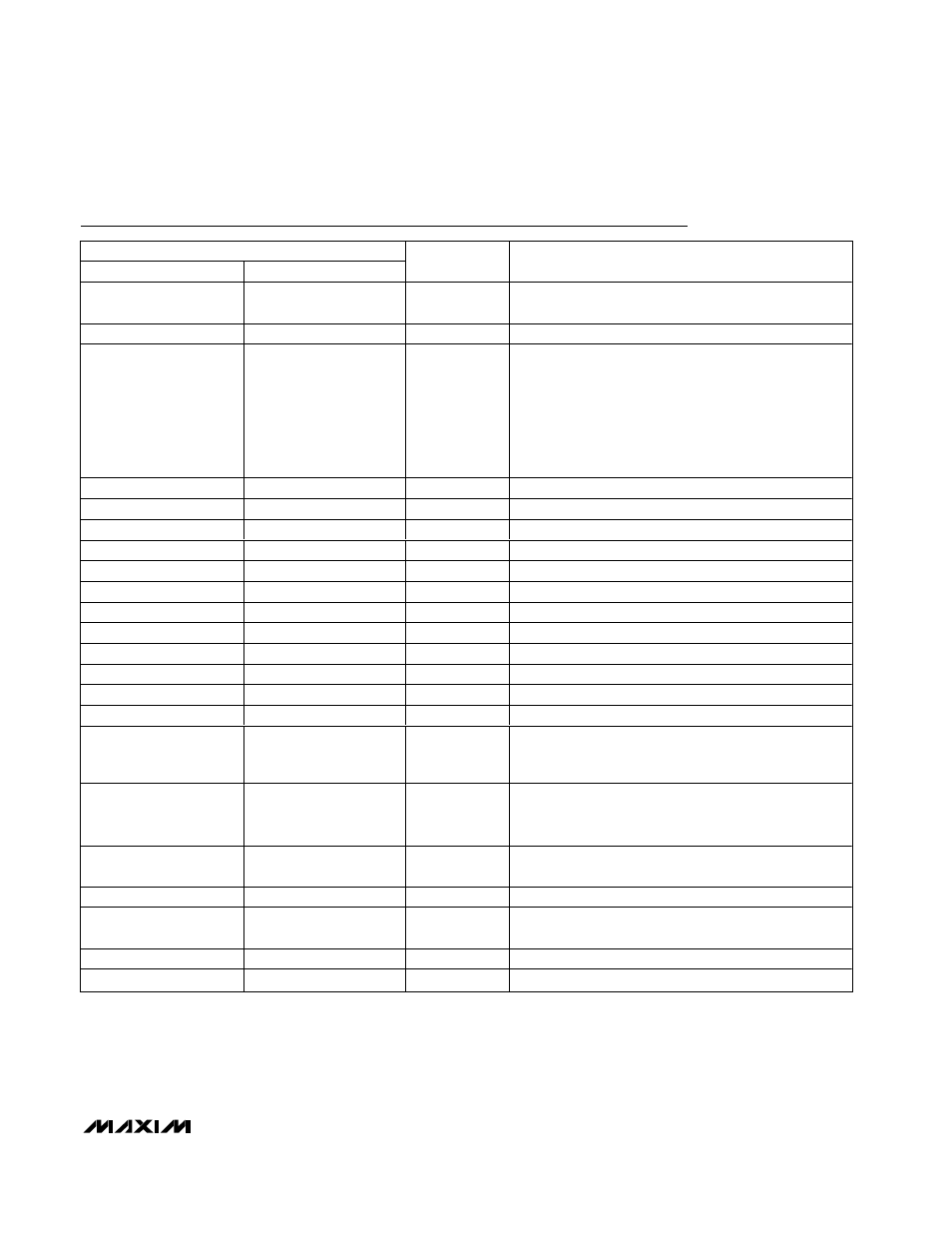
Pin Description
PIN
TSSOP
QFN
NAME
FUNCTION
1, 2, 4, 5, 45, 46, 47
39, 40, 41, 43, 44, 46, 47
RxOUT14–
RxOUT20
Channel 2 Single-Ended Outputs
3, 25, 32, 38, 44
19, 26, 32, 38, 45
GND
Ground
6
48
DCB/NC
LVTTL/LVCMOS DC-Balance Programming Input:
MAX9210: pulled up to V
CC
MAX9212: pulled down to GND
MAX9214: pulled up to V
CC
MAX9216: pulled down to GND
MAX9220: pulled up to V
CC
MAX9222: pulled up to V
CC
See Table 1.
7, 13, 18
1, 7, 12
LVDS GND
LVDS Ground
8
2
RxIN0-
Inverting Channel 0 LVDS Serial Data Input
9
3
RxIN0+
Noninverting Channel 0 LVDS Serial Data Input
10
4
RxIN1-
Inverting Channel 1 LVDS Serial Data Input
11
5
RxIN1+
Noninverting Channel 1 LVDS Serial Data Input
12
6
LVDS V
CC
LVDS Supply Voltage
14
8
RxIN2-
Inverting Channel 2 LVDS Serial Data Input
15
9
RxIN2+
Noninverting Channel 2 LVDS Serial Data Input
16
10
RxCLK IN-
Inverting LVDS Parallel Rate Clock Input
17
11
RxCLK IN+
Noninverting LVDS Parallel Rate Clock Input
19, 21
13, 15
PLL GND
PLL Ground
20
14
PLL V
CC
PLL Supply Voltage
22
16
PWRDWN
5V Tolerant LVTTL/LVCMOS Power-Down Input. Internally
pulled down to GND. Outputs are high impedance when
PWRDWN = low or open.
23
17
RxCLK OUT
Parallel Rate Clock Single-Ended Output.
MAX9210/MAX9212/MAX9214/MAX9216, rising edge
strobe. MAX9220/MAX9222, falling edge strobe.
24, 26, 27, 29, 30, 31, 33
18, 20, 21, 23, 24, 25, 27
RxOUT0–
RxOUT6
Channel 0 Single-Ended Outputs
28, 36, 48
22, 30, 42
V
CCO
Output Supply Voltage
34, 35, 37, 39, 40, 41, 43
28, 29, 31, 33, 34, 35, 37
RxOUT7–
RxOUT13
Channel 1 Single-Ended Outputs
42
36
V
CC
Digital Supply Voltage
—
EP
EP
Exposed Paddle. Solder to ground.