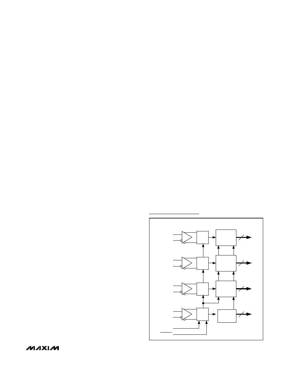
Functional diagram – Rainbow Electronics MAX9216 User Manual
Page 13
5V Tolerant Input
PWRDWN is 5V tolerant and is internally pulled down to
GND. DCB/NC is not 5V tolerant. The input voltage
range for DCB/NC is nominally ground to V
CC
.
Normally, DCB/NC is connected to V
CC
or ground.
Skew Margin (RSKM)
Skew margin (RSKM) is the time allowed for degrada-
tion of the serial data sampling setup and hold times by
sources other than the deserializer. The deserializer
sampling uncertainty is accounted for and does not
need to be subtracted from RSKM. The main outside
contributors of jitter and skew that subtract from RSKM
are interconnect intersymbol interference, serializer
pulse position uncertainty, and pair-to-pair path skew.
V
CCO
Output Supply and Power Dissipation
The outputs have a separate supply (V
CCO
) for interfac-
ing to systems with 1.8V to 5V nominal input logic levels.
The DC Electrical Characteristics table gives the maxi-
mum supply current for V
CCO
= 3.6V with 8pF load at
several switching frequencies with all outputs switching in
the worst-case switching pattern. The approximate incre-
mental supply current for V
CCO
other than 3.6V with the
same 8pF load and worst-case pattern can be calculated
using:
I
I
= C
T
V
I
0.5f
C
x 21 (data outputs)
+ C
T
V
I
f
C
x 1 (clock output)
where:
I
I
= incremental supply current
C
T
= total internal (C
INT
) and external (C
L
) load capaci-
tance
V
I
= incremental supply voltage
f
C
= output clock switching frequency
The incremental current is added to (for V
CCO
> 3.6V)
or subtracted from (for V
CCO
< 3.6V) the DC Electrical
Characteristics table maximum supply current. The
internal output buffer capacitance is C
INT
= 6pF. The
worst-case pattern switching frequency of the data out-
puts is half the switching frequency of the output clock.
In the following example, the incremental supply current is
calculated for V
CCO
= 5.5V, f
C
= 34MHz, and C
L
= 8pF:
V
I
= 5.5V - 3.6V = 1.9V
C
T
= C
INT
+ C
L
= 6pF + 8pF = 14pF
where:
I
I
= C
T
V
I
0.5F
C
x 21 (data outputs) + C
T
V
I
f
C
x 1 (clock
output)
I
I
= (14pF x 1.9V x 0.5 x 34MHz x 21) + (14pF x 1.9V x
34MHz)
I
I
= 9.5mA + 0.9mA = 10.4mA
The maximum supply current in DC-balanced mode for
V
CC
= V
CCO
= 3.6V at f
C
= 34MHz is 106mA (from the
DC Electrical Characteristics table). Add 10.4mA to get
the total approximate maximum supply current at V
CCO
= 5.5V and V
CC
= 3.6V.
If the output supply voltage is less than V
CCO
= 3.6V,
the reduced supply current can be calculated using the
same formula and method.
At high switching frequency, high supply voltage, and
high capacitive loading, power dissipation can exceed
the package power dissipation rating. Do not exceed
the maximum package power dissipation rating. See
the Absolute Maximum Ratings for maximum package
power dissipation capacity and temperature derating.
Rising- or Falling-Edge Output Strobe
The MAX9210/MAX9212/MAX9214/MAX9216 have a
rising-edge output strobe, which latches the parallel
output data into the next chip on the rising edge of
RxCLK OUT. The MAX9220/MAX9222 have a falling-
edge output strobe, which latches the parallel output
data into the next chip on the falling edge of RxCLK
OUT. The deserializer output strobe polarity does not
need to match the serializer input strobe polarity. A
deserializer with rising or falling edge output strobe can
be driven by a serializer with a rising edge input strobe.
MAX9210/MAX9212/MAX9214/MAX9216/MAX9220/MAX9222
Programmable DC-Balance
21-Bit Deserializers
______________________________________________________________________________________
13
RxIN0+
LVDS DATA
RECEIVER 0
RxIN0-
STROBE
DATA
CHANNEL 0
RxOUT0–6
SERIAL-TO-
PARALLEL
CONVERTER
RxIN1+
LVDS DATA
RECEIVER 1
RxIN1-
STROBE
DATA
CHANNEL 1
RxOUT7–13
SERIAL-TO-
PARALLEL
CONVERTER
RxIN2+
LVDS DATA
RECEIVER 2
RxIN2-
STROBE
DATA
CHANNEL 2
RxOUT14–20
SERIAL-TO-
PARALLEL
CONVERTER
RxCLK IN+
LVDS CLOCK
RECEIVER
RxCLK IN-
DCB/NC
7x/9x
PLL
RxCLK OUT
REFERENCE
CLOCK
GENERATOR
PWRDWN
Functional Diagram