Typical operating characteristics, Ac electrical characteristics (continued) – Rainbow Electronics MAX9216 User Manual
Page 4
WORST-CASE PATTERN SUPPLY CURRENT
vs. FREQUENCY
MAX9210 toc01
FREQUENCY (MHz)
SUPPLY CURRENT (mA)
65
50
35
20
60
80
100
120
140
160
40
5
80
MAX9214
DC-BALANCED MODE
WORST-CASE PATTERN SUPPLY CURRENT
vs. FREQUENCY
MAX9210 toc02
FREQUENCY (MHz)
SUPPLY CURRENT (mA)
75
90
60
30
45
60
80
100
120
160
40
15
140
MAX9214
NON-DC-BALANCED MODE
OUTPUT TRANSITION TIME
vs. OUTPUT SUPPLY VOLTAGE (V
CCO
)
MAX9210 toc03
OUTPUT SUPPLY VOLTAGE (V)
OUTPUT TRANSITION TIME (ns)
4.5
4.0
3.5
3.0
2
3
4
5
1
2.5
5.0
MAX9214
NON-DC-BALANCED MODE
t
F
t
R
MAX9210/MAX9212/MAX9214/MAX9216/MAX9220/MAX9222
Programmable DC-Balance
21-Bit Deserializers
4
_______________________________________________________________________________________
AC ELECTRICAL CHARACTERISTICS (continued)
(V
CC
= V
CCO
= +3.0V to 3.6V, 100mV
P-P
at 200kHz supply noise, C
L
= 8pF, PWRDWN = high, DCB/NC = high or low, differential
input voltage
V
ID
= 0.1V to 1.2V, input common-mode voltage V
CM
=
V
ID
/2
to 2.4V - V
ID
/2
, T
A
= -40°C to +85°C, unless other-
wise noted. Typical values are at V
CC
= V
CCO
= +3.3V,
V
ID
= 0.2V, V
CM
= 1.25V, T
A
= 25°C.) (Notes 3, 4, 5)
PARAMETER
SYMBOL
CONDITIONS
MIN
TYP
MAX
UNITS
RxCLK OUT High Time
RCOH
Figures 5a, 5b
0.35 x
RCOP
0.4 x
RCOP
ns
RxCLK OUT Low Time
RCOL
Figures 5a, 5b
0.35 x
RCOP
0.44 x
RCOP
ns
RxOUT Setup to RxCLK OUT
RSRC
Figures 5a, 5b
0.30 x
RCOP
0.35 x
RCOP
ns
RxOUT Hold from RxCLK OUT
RHRC
Figures 5a, 5b
0.45 x
RCOP
0.48 x
RCOP
ns
RxCLK IN to RxCLK OUT Delay
RCCD
Figures 6a, 6b
4.9
6.17
8.1
ns
Deserializer Phase-Locked
Loop Set
RPLLS
Figure 7
32800 x
RCIP
ns
Deserializer Power-Down Delay
RPDD
Figure 8
100
ns
Note 1: Current into a pin is defined as positive. Current out of a pin is defined as negative. All voltages are referenced to ground
except V
TH
and V
TL
.
Note 2: Maximum and minimum limits over temperature are guaranteed by design and characterization. Devices are production
tested at T
A
= +25°C.
Note 3: AC parameters are guaranteed by design and characterization, and are not production tested. Limits are set at ±6 sigma.
Note 4: C
L
includes probe and test jig capacitance.
Note 5: RCIP is the period of RxCLK IN. RCOP is the period of RxCLK OUT. RCIP = RCOP.
Note 6: RSKM measured with
≤
150ps cycle-to-cycle jitter on RxCLK IN.
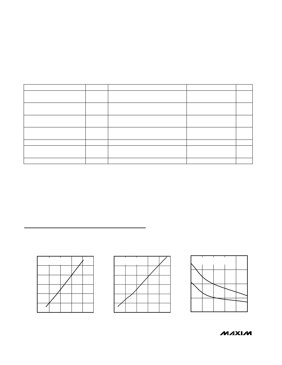
Typical Operating Characteristics
(V
CC
= V
CCO
= +3.3V, C
L
= 8pF, PWRDWN = high, differential input voltage
V
ID
= 0.2V, input common-mode voltage V
CM
= 1.2V,
T
A
= +25°C, unless otherwise noted.)