Rainbow Electronics MAX9216 User Manual
Page 2
MAX9210/MAX9212/MAX9214/MAX9216/MAX9220/MAX9222
Programmable DC-Balance
21-Bit Deserializers
2
_______________________________________________________________________________________
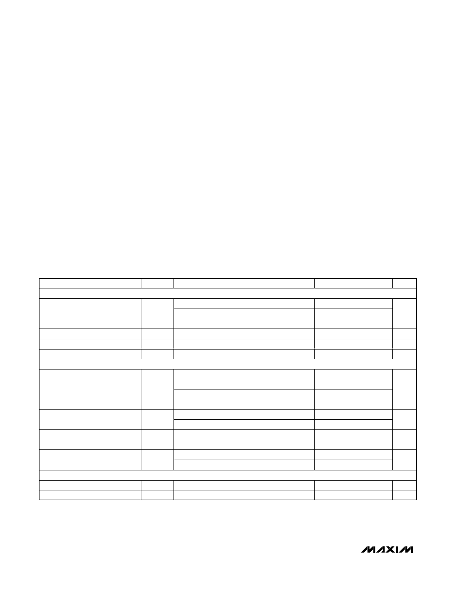
ABSOLUTE MAXIMUM RATINGS
DC ELECTRICAL CHARACTERISTICS
(V
CC
= +3.0V to +3.6V, V
CCO
= +3.0V to +5.5V, PWRDWN = high, DCB/NC = high or low, differential input voltage
V
ID
= 0.05V to
1.2V, input common-mode voltage V
CM
=
V
ID
/2
to 2.4V - V
ID
/2
, T
A
= -40°C to +85°C, unless otherwise noted. Typical values are
at V
CC
= V
CCO
= +3.3V,
V
ID
= 0.2V, V
CM
= 1.25V, T
A
= +25°C.) (Notes 1, 2)
Stresses beyond those listed under “Absolute Maximum Ratings” may cause permanent damage to the device. These are stress ratings only, and functional
operation of the device at these or any other conditions beyond those indicated in the operational sections of the specifications is not implied. Exposure to
absolute maximum rating conditions for extended periods may affect device reliability.
V
CC
to GND ...........................................................-0.5V to +4.0V
V
CCO
to GND.........................................................-0.5V to +6.0V
RxIN_, RxCLK IN_ to GND ....................................-0.5V to +4.0V
PWRDWN to GND .................................................-0.5V to +6.0V
DCB/NC to GND.........................................-0.5V to (V
CC
+ 0.5V)
RxOUT_, RxCLK OUT to GND .................-0.5V to (V
CCO
+ 0.5V)
Continuous Power Dissipation (T
A
= +70
°
C)
48-Pin TSSOP (derate 16mW/
°
C above +70
°
C) ........ 1282mW
48-Lead Thin QFN
(derate 26.3mW/
°
C above +70
°
C) ................................2105mW
Storage Temperature Range..............................-65
°
C to +150
°
C
Junction Temperature ......................................................+150
°
C
ESD Protection
Human Body Model (R
D
= 1.5k
Ω, C
S
= 100pF)
All Pins to GND ................................................................±5kV
IEC 61000-4-2 (R
D
= 330
Ω, C
S
= 150pF) Level 4
Contact Discharge LVDS Inputs (RxIN_, RxCLK IN_)
to GND .............................................................................±8kV
Air Discharge LVDS Inputs (RxIN_, RxCLK IN_)
to GND ...........................................................................±15kV
Lead Temperature (soldering, 10s) .................................+300
°
C
PARAMETER
SYMBOL
CONDITIONS
MIN
TYP
MAX
UNITS
SINGLE-ENDED INPUTS (PWRDWN, DCB/NC)
PWRDWN
2.0
5.5
High-Level Input Voltage
V
IH
DCB/NC
2.0
V
CC
+
0.3
V
Low-Level Input Voltage
V
IL
-0.3
+0.8
V
Input Current
I
IN
V
IN
= high or low,
PWRDWN = high or low
-20
+20
µA
Input Clamp Voltage
V
CL
I
CL
= -18mA
-1.5
V
SINGLE-ENDED OUTPUTS (RxOUT_, RxCLK OUT)
I
OH
= -100µA
V
CCO
-
0.1
High-Level Output Voltage
V
OH
I
OH
= -2mA
V
CCO
-
0.25
V
I
OL
= 100µA
0.1
Low-Level Output Voltage
V
OL
I
OL
= 2mA
0.2
V
High-Impedance Output Current
I
OZ
PWRDWN = low, V
OUT_
= -0.3V to
(V
CCO
+ 0.3V)
-20
+20
µA
V
CCO
= 3.0V to 3.6V, V
OUT
= 0V
-10
-40
Output Short-Circuit Current
Note: Short one output at a time.
I
OS
V
CCO
= 4.5V to 5.5V, V
OUT
= 0V
-28
-75
mA
LVDS INPUTS
Differential Input High Threshold
V
TH
50
mV
Differential Input Low Threshold
V
TL
-50
mV