U3745bm, Electrical characteristics (continued), Electrical characteristics – Rainbow Electronics U3745BM User Manual
Page 25
25
U3745BM
4663A–RKE–06/03
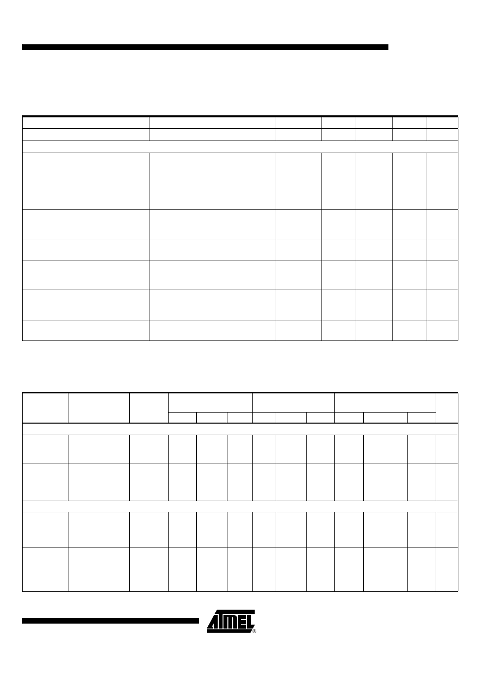
Threshold voltage for reset
V
ThRESET
1.95
2.8
3.75
V
Digital Ports
Data output
- Saturation voltage LOW
- Internal pull-up resistor
- Maximum time constant
- Maximum capacitive load
I
ol
= 1 mA
t
= C
L
(R
pup
//R
Ext
)
without ext. pull-up resistor
R
ext
= 5 k
W
V
OI
R
Pup
t
C
L
C
L
39
0.08
50
0.3
61
2.5
41
540
V
k
W
µs
pF
pF
POUT output
- Saturation voltage LOW
- Saturation voltage HIGH
I
POUT
= 1 mA
I
POUT
= -1 mA
V
Ol
V
Oh
V
S
-0.3V
0.08
V
S
-0.14V
0.3
V
V
ASK input
- High-level input voltage
ASK
V
Ih
0.8
´
V
S
V
ENABLE input
- Low-level input voltage
- High-level input voltage
Idle mode
Active mode
V
Il
V
Ih
0.8
´
V
S
0.2
´
V
S
V
V
MODE input
- Low-level input voltage
- High-level input voltage
Division factor = 10
Division factor = 14
V
Il
V
Ih
0.8
´
V
S
0.2
´
V
S
V
V
TEST input
- Low-level input voltage
Test input must always be set to LOW
V
Il
0.2
´
V
S
V
Electrical Characteristics (Continued)
All parameters refer to GND, V
S
= 5 V, T
amb
= 25
°
C, f
0
= 433.92 MHz and f
0
= 315 MHz, unless otherwise specified. The
possible operating range refer to different circuit conditions: V
S
= 4.5 V to 5.5 V, T
amb
= -40
°
C to +85
°
C
Parameters
Test Conditions
Symbol
Min.
Typ.
Max.
Unit
Electrical Characteristics
All parameters refer to GND, V
S
= 5 V, T
amb
= 25
°
C, f
0
= 433.92 MHz and f
0
= 315 MHz, unless otherwise specified. The
possible operating range refer to different circuit conditions: V
S
= 4.5 V to 5.5 V, T
amb
= -40
°
C to +85
°
C
Parameter
Test Condition
Symbol
6.76438-Mhz Osc.
(Mode 1)
4.90625-Mhz Osc.
(Mode 0)
Variable Oscillator
Unit
Min.
Typ.
Max.
Min.
Typ.
Max.
Min.
Typ.
Max.
Basic Clock Cycle of the Digital Circuitry
Basic clock
cycle
MODE = 0 (USA)
MODE = 1
(Europe)
T
Clk
2.0697
2.0383
1/(f
XTO
/10)
1/(f
XTO
/14)
µs
µs
Extended
basic clock
cycle
BR_Range0
BR_Range1
BR_Range2
BR_Range3
T
XClk
16.6
8.3
4.1
2.1
16.3
8.2
4.1
2.0
8
´
T
Clk
4
´
T
Clk
2
´
T
Clk
1
´
T
Clk
µs
µs
µs
µs
Polling Mode
Sleep time
Sleep and XSleep
are defined in the
OPMODE register
T
Sleep
Sleep
´
X
Sleep
´
1024
´
2.0697
Sleep
´
X
Sleep
´
1024
´
2.0383
Sleep
´
X
Sleep
´
1024
´
T
Clk
ms
Start-up time
BR_Range0
BR_Range1
BR_Range2
BR_Range3
T
Startup
1855
1061
1061
663
1827
1045
1045
653
896.5
512.5
512.5
320.5
´
T
Clk
µs
µs
µs
µs