U3745bm – Rainbow Electronics U3745BM User Manual
Page 12
12
U3745BM
4663A–RKE–06/03
XSleep
Temp
= 1 implies the temporary extension factor. The extended sleep time is used
as long as every bit check is OK. If the bit check fails once, this bit is set back to 0 auto-
matically resulting in a regular sleep time. This functionality can be used to save current
in presence of a modulated disturber similar to an expected transmitter signal. The con-
nected microcontroller is rarely activated in that condition. If the disturber disappears,
the receiver switches back to regular polling and is again sensitive to appropriate trans-
mitter signals.
According to Table 7, the highest register value of Sleep sets the receiver to a perma-
nent sleep condition. The receiver remains in that condition until another value for Sleep
is programmed into the OPMODE register. This function is desirable where several
devices share a single data line.
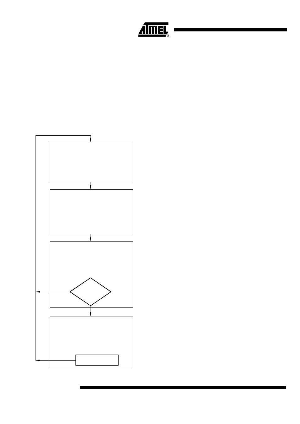
Figure 7. Polling Mode Flow Chart
Sleep mode:
All circuits for signal processing
are disabled. Only XTO and
polling logic are enabled.
T
Sleep
= Sleep x X
Sleep
x 1024 x T
Clk
Start-up mode:
The signal processing circuits are
enabled. After the start-up time
(T
Startup
) all circuits are in stable
condition and ready to receive.
Bit check mode:
The incomming data stream is
analyzed. If the timing indicates a
valid transmitter signal, the receiver
is set to receiving mode. Otherwise
it is set to Sleep mode.
Receiving mode:
The receiver is turned on
permanently and passes the data
stream to the connected
m
C. It can
be set to Sleep mode through an
OFF command via pin DATA or
ENABLE.
Bitcheck
OK ?
OFF command
5-bit word defined by Sleep0 to
Sleep4 in OPMODE register
Extension factor defined by XSleep
Temp
according to Table 8
NO
YES
Sleep:
X
Sleep
:
T
Clk
:
T
Startup
:
I
S
= I
SON
I
S
= I
SON
T
Startup
I
S
= I
SON
T
Bitcheck
I
S
= I
SON
Basic clock cycle defined by f
XTO
and Pin MODE
Is defined by the selected baud rate
range and T
Clk
. The baud rate range
is defined by Baud0 and Baud1 in
the OPMODE register.
T
Bitcheck
:
Depends on the result of the bitcheck
If the bitcheck is ok, T
Bitcheck
depends on
the number of bits to be
checked (N
Bitchecked
) and on the
utilized data rate.
If the bitcheck fails, the average
time period for that check depends
on the selected baud rate range and
on T
Clk
.The baud rate range is
defined by Baud0 and Baud1 in the
OPMODE register.