Th7834c – Rainbow Electronics TH7834C User Manual
Page 9
9
TH7834C
1997A–IMAGE–05/02
Note:
1. For ¼ of total CCD register.
Note:
The maximum clock frequency is limited by the dark signal increase. Full performance for 5 MHz.
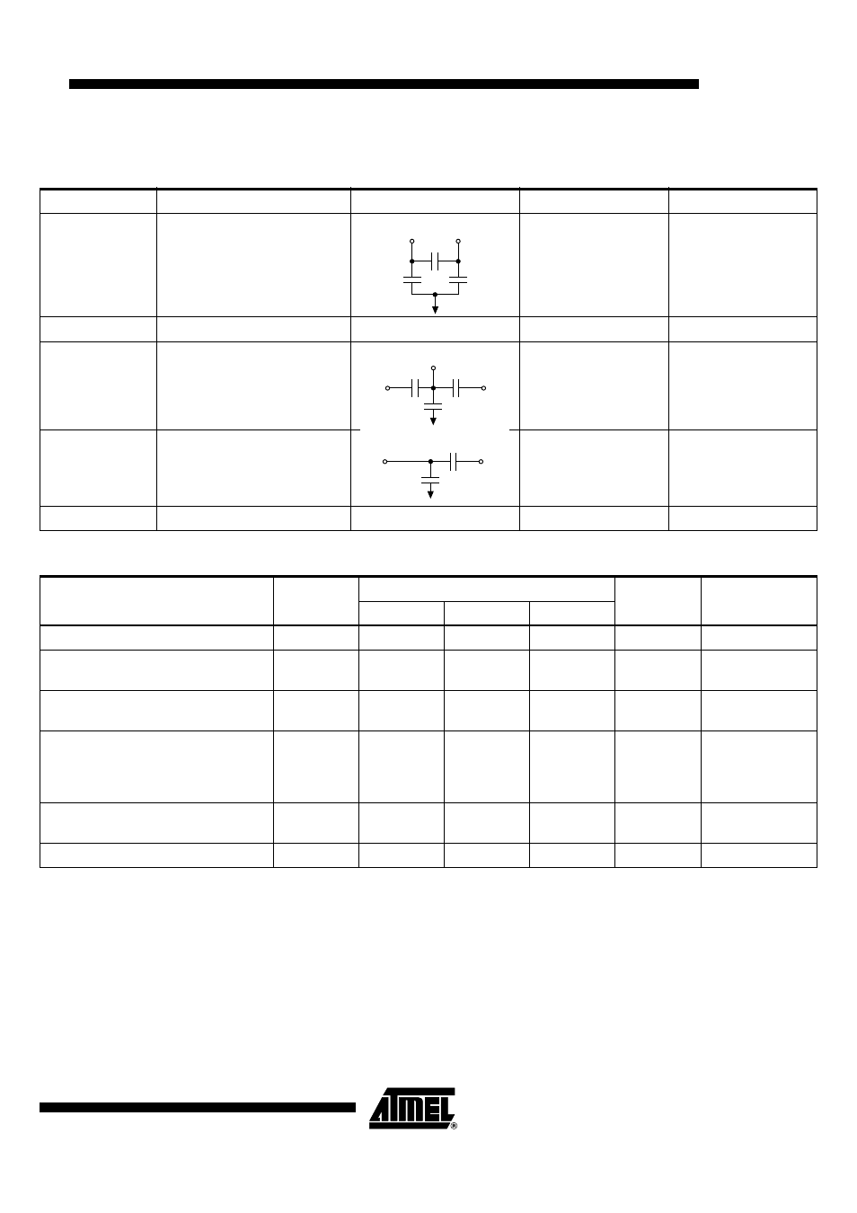
Table 4. Drive Clock Capacitances Operating Frequencies
Symbol
Function/Clock
Capacitive Network
Total
Max. Frequency
Φ
L1
,
Φ
L2
Register Main Transport Clock
Φ
L1
: 570 pF
Φ
L2
: 640 pF
for one CCD
10 MHz
Φ
LS1-2
,
Φ
LS3-4
Register End Transfer Clock
≤
50 pF per phase
10 MHz
Φ
P1-2
,
Φ
P3-4
Transfer Clock
80 pF per phase
Pulse duration
≥
2 µs
Period:
≥
608.6 µs
(4 outputs mode)
Φ
A1-2
,
Φ
A3-4
Antiblooming And Exposure
Time Control
100 pF per phase
Φ
R1-2
,
Φ
R3-4
Reset Clock
≤
50 pF per phase
10 MHz
Φ
L1
Φ
L2
160pF
250pF
320pF
Φ
P
Φ
L2
15pF
VSS
VST
15pF
50pF
Φ
A
15pF
VSS
VST
60pF
Table 5. Static and Dynamic Electrical Characteristics
Parameter
Symbol
Value
Unit
Remarks
Min.
Typ.
Max.
DC Output Level (Pins: 1, 28, 29, 56)
V
ref
10
V
Output Impedance (Pins: 1, 28, 29,
56)
Z
S
400
600
Ω
Maximum Data Output Frequency
Per Channel
F
S
max
5
10
MHz
Input Current On Active Pins 4, 6, 7,
8, 10, 11, 12, 13, 16, 17, 18, 19, 21,
23, 32, 34, 35, 36, 38, 39, 40, 41, 44,
45, 46, 47, 49, 51
I
e
<< 1
2
µA
V
in
= 15V
with all other
pins = 0V
Amplifier Drain Supply Current (Per
V
DD
)
I
DD1-2
, I
DD3-4
10
16
mA
V
DD
= 15V
Static Power Dissipation (Per V
DD
)
P
D1-2
, P
D3-4
165
240
mW