Operating precautions, Operating conditions (t = 25˚c), Timing diagram – Rainbow Electronics TH7834C User Manual
Page 6: Th7834c, Operating conditions (t = 25°c)
6
TH7834C
1997A–IMAGE–05/02
Operating
Precautions
Shorting the video outputs to VSS or VDD, even temporarily, can permanently damage
the output amplifiers.
Operating Conditions (T = 25°C)
Note:
If no exposure time control is required,
Φ
A1-2
and
Φ
A3-4
must be connected to an adjustable DC bias (see Figure 7).
Typical current in V
DR
, V
A
< 10 µA; in V
GS
, V
ST
< 1 µA.
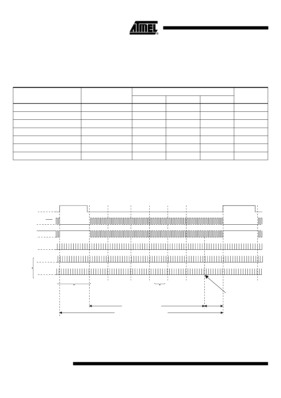
Timing Diagram
Figure 3. Line Timing Diagram
•
Minimum exposure time: Ti min = readout time.
For data rate of 5 MHz: Ti min =
= 608.6 µs.
Note:
It is better to clean the shift registers (with running clocks) and not to stop clocking them
after readout time.
Table 1. DC Characteristics
Parameter
Symbol
Value
Unit
Min.
Typ.
Max.
Output Amplifier Drain Supply
V
DD1-2
, V
DD3-4
14.5
15
15.5
V
Substrate Voltage
V
SS
0
0
V
Reset DC Bias
V
DR1
, V
DR2
, V
DR3
, V
DR4
V
DD
- 0.5
V
Output Amplifier Source Bias
V
S1
, V
S2
, V
S3
, V
S4
0
V
Output Gate DC Bias
V
GS1-2
, V
GS3-4
2.2
2.4
2.6
V
Photosensitive Zone DC Bias
V
ST
3.5
4
4.5
V
Antiblooming Diode Bias
VA
1-2
, VA
3-4
14
14.5
15
V
Φ
P3-4
Φ
P1-2
Φ
Φ
LS1-2,
LS3-4
Φ
Φ
R1-2,
R3-4
Φ
Ec1
(clamp)
External
Φ
Ech
(Sampling)
Detailed timing diagram
for transfert from
photosite to register
(see fig. 4)
Detailed pixel
timing diagram
(see fig. 5)
Φ
Φ
L1,
L2
Readout time for line M
Cleaning
Pixel N
Integration time Ti for line M+1
3043
5 MHz
-----------------