Description, Th7834c, Pin description (continued) – Rainbow Electronics TH7834C User Manual
Page 3
3
TH7834C
1997A–IMAGE–05/02
Notes:
1. Pins
Φ
A1-2
, V
GS1-2
,
Φ
P1-2
, VA
1-2
,
Φ
LS1-2
, V
DD1-2
,
Φ
R1-2
and respectively,
Φ
A3-4
, V
GS3-4
,
Φ
P3-4
, VA
3-4,
Φ
LS3-4
, V
DD3-4
,
Φ
R3-4
are not
connected together inside the package.
2. Two Pins V
ST
connected together inside the package.
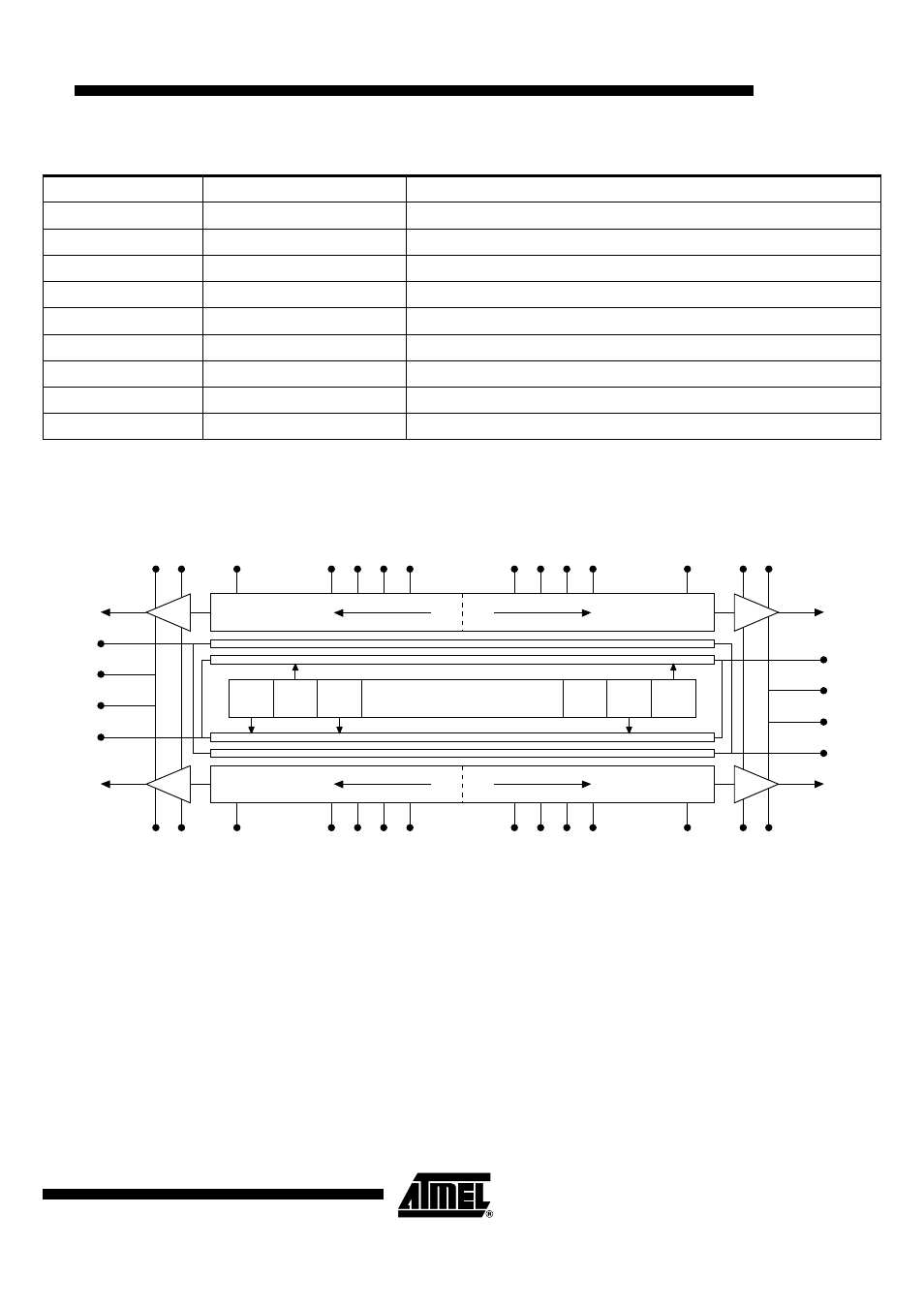
Figure 1. TH7834 Block Diagram
Description
TH7834C high resolution linear array consists of 12000 useful pixel photosensitive line,
associated with four CCD shift registers and four output amplifiers. Transfer gates on
both sides of the photosensitive line enable delivery of charges, respectively:
•
on one side, charge accumulated by odd pixels (1, 3, 5… 11999), to CCD shift
registers A and C,
•
on the other side, charge accumulated by even pixels (2, 4, 6… 12000), to CCD
shift registers B and D.
Shift registers 1 and 2 collect charges generated by one half of the photosensitive line
(pixel 1 to 6000), whereas shift registers 3 and 4 collect charges generated by the sec-
ond half of the photosensitive line (pixels 12000 to 6001).
46
Φ
1B
Register Main Transport Clock
47
Φ
3B
Register Main Transport Clock
49
Φ
P1-2
Transfer Clock
50
VA
1-2
Antiblooming Diode Bias
51
Φ
LS1-2
Register End Transport Clock
53
V
DD1-2
Amplifier Drain Supplies (Outputs 1, 2)
54
V
S2
Amplifier Source Bias (Output 2)
55
V
DR2
Reset DC Bias (Output 2)
56
V
OS2
Output 2 (Even Pixels)
Pin Description (Continued)
Pin Number
Symbol
Designation
Φ
2B
Φ
2A
Φ
LS1-2
VDR2
VDR4
VS2
VS4
Φ
P1-2
VDD1-2
Φ
R1-2
Φ
P3-4
VDD3-4
Φ
R3-4
VST
VST
VGS1-2
VDR1
VDR3
VS1
VS3
VOS1
VOS3
CCD A
CCD C
VOS2
VOS4
CCD B
1
CCD D
12000
Φ
3D
Φ
3C
VGS3-4
Φ
LS3-4
Φ
4B
Φ
4A
Φ
1D
Φ
1C
Φ
1B
Φ
1A
Φ
4D
Φ
4C
Φ
3B
Φ
3A
Φ
2D
Φ
2C